


رقم الموديل WEP002004C
◄النوع: الحرف
◄الهيكل: COG+FR+PCB
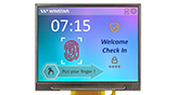
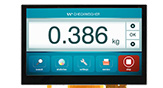
◄20 حرف × 4 سطور
◄وحدة تحكم مدمجة SSD1311
◄مزود طاقة 3.3V/5V فولت
◄1/32 حمولة
◄الواجهة: 6800/8080/SPI/I2C
◄ون العرض:أبيض / أصفر
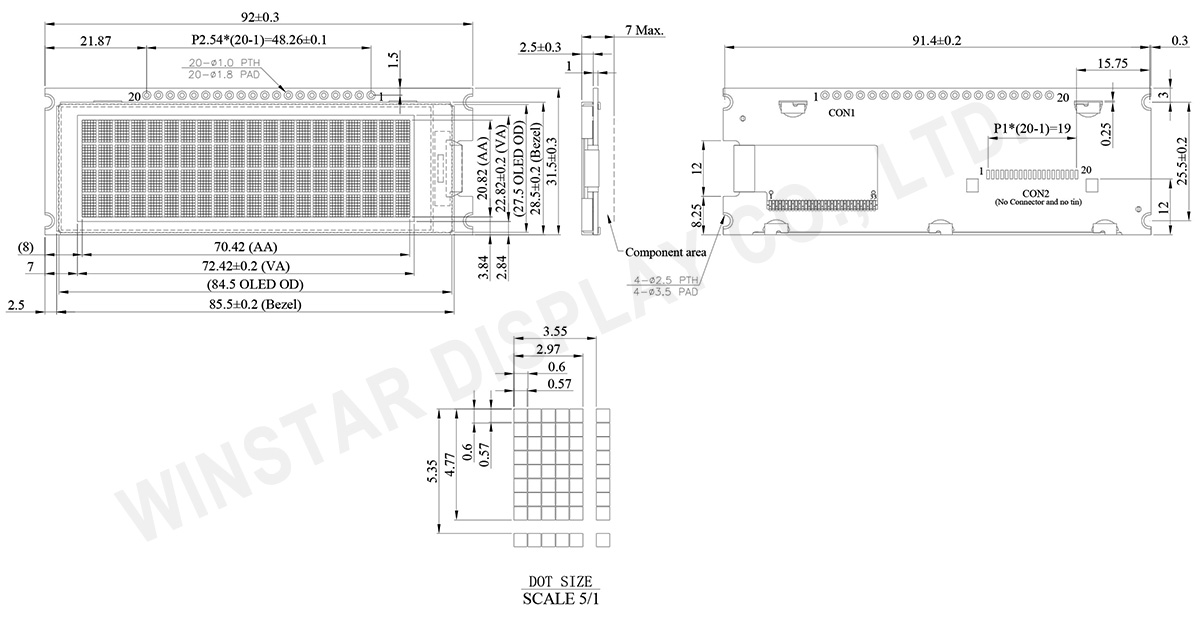
الرسم
المواصفات
وظيفة دبوس واجهة التوصيل
| Pin No. | الرمز | Pin Type | الوصف | ||||||||||||||||||
|---|---|---|---|---|---|---|---|---|---|---|---|---|---|---|---|---|---|---|---|---|---|
| 1 | VSS | P | Ground | ||||||||||||||||||
| 2 | VDD | P | Power supply and power supply for interface logic level. | ||||||||||||||||||
| 3 | REGVDD | I | Internal VDD regulator selection pin in 5V I/O application mode. When this pin is pulled HIGH, internal VDD regulator is enabled (5V I/O application). When this pin is pulled LOW, internal VDD regulator is disabled (Low voltage I/O application). |
||||||||||||||||||
| 4 | D/C# | I | This pin is Data/Command control pin connecting to the MCU. When the pin is pulled HIGH, the data at D[7:0] will be interpreted as data. When the pin is pulled LOW, the data at D[7:0] will be transferred to a command register. In I2C mode, this pin acts as SA0 for slave address selection. When serial interface is selected, this pin must be connected to VSS. |
||||||||||||||||||
| 5 | R/W# (WR#) | I | This pin is read / write control input pin connecting to the MCU interface. When 6800 interface mode is selected, this pin will be used as Read/Write (R/W#) selection input. Read mode will be carried out when this pin is pulled HIGH and write mode when LOW. When 8080 interface mode is selected, this pin will be the Write (WR#) input. Data write operation is initiated when this pin is pulled LOW and the chip is selected. When serial or I2C interface is selected, this pin must be connected to VSS. |
||||||||||||||||||
| 6 | E/RD# | I | This pin is MCU interface input. When 6800 interface mode is selected, this pin will be used as the Enable (E) signal. Read/write operation is initiated when this pin is pulled HIGH and the chip is selected. When 8080 interface mode is selected, this pin receives the Read (RD#) signal. Read operation is initiated when this pin is pulled LOW and the chip is selected. When serial or I2C interface is selected, this pin must be connected to VSS. |
||||||||||||||||||
| 7 | D0 | I/O | These pins are bi-directional data bus connecting to the MCU data bus. Unused pins are recommended to tie LOW. When serial interface mode is selected, D0 will be the serial clock input: SCLK; D1 will be the serial data input: SID and D2 will be the serial data output: SOD. When I2C mode is selected, D2, D1 should be tied together and serve as SDAout, SDAin in application and D0 is the serial clock input, SCL. |
||||||||||||||||||
| 8 | D1 | ||||||||||||||||||||
| 9 | D2 | ||||||||||||||||||||
| 10 | D3 | ||||||||||||||||||||
| 11 | D4 | ||||||||||||||||||||
| 12 | D5 | ||||||||||||||||||||
| 13 | D6 | ||||||||||||||||||||
| 14 | D7 | ||||||||||||||||||||
| 15 | CS# | I | This pin is the chip select input connecting to the MCU. The chip is enabled for MCU communication only when CS# is pulled LOW (active LOW). In I2C mode, this pin must be connected to VSS. |
||||||||||||||||||
| 16 | RES# | I | This pin is reset signal input. When the pin is pulled LOW, initialization of the chip is executed. Keep this pin pull HIGH during normal operation. |
||||||||||||||||||
| 17 | BS0 | I | setting as described in the following table. BS2, BS1 and BS0 are pin select. Bus Interface selection
(1) 0 is connected to VSS (2) 1 is connected to VDD |
||||||||||||||||||
| 18 | BS1 | ||||||||||||||||||||
| 19 | BS2 | ||||||||||||||||||||
| 20 | VSS (FRGnd) |
P | Ground |
البيانات الميكانيكية
| العنصر | الأبعاد | الوحدة |
|---|---|---|
| تنسيق العرض | 20 حرف × 4 سطور | - |
| أبعاد الوحدة | 92.0 × 31.5 × 7.0 Max | mm |
| منطقة العرض | 72.42 × 22.82 | mm |
| منطقة نشطة | 70.42 × 20.82 | mm |
| حجم النقطة | 0.57 × 0.57 | mm |
| درجة النقطة | 0.60 × 0.60 | mm |
| حجم الحرف | 2.97 × 4.77 | mm |
| Character pitch | 3.55 × 5.35 | mm |
| نوع شاشة LCD | OLED , Monochrome | |
| Duty | 1/32 | |
| IC | SSD1311 | |
| الواجهة | 6800, 8080, SPI, I2C | |
| الحجم | 2.89 بوصة | |
تصنيفات الحد الأقصى المطلق
| العنصر | الرمز | أدنى قيمة | أقصى قيمة | الوحدة |
|---|---|---|---|---|
| درجة حرارة التشغيل | TOP | -40 | +80 | °C |
| درجة حرارة التخزين | TST | -40 | +85 | °C |
| Supply Voltage For Logic | VDD-VSS | -0.3 | 5.5 | V |
المميزات الإلكترونية
DC المميزات الإلكترونية
| العنصر | الرمز | الحالة | أدنى قيمة | القيمة النموذجية | أقصى قيمة | الوحدة |
|---|---|---|---|---|---|---|
| Supply Voltage For Logic | VDD-VSS | - | 4.8 | 5.0 | 5.3 | V |
| Input High Volt. | VIH | - | 0.8xVDD | - | VDD | V |
| Input Low Volt. | VIL | - | GND | - | 0.2xVDD | V |
| Output High Volt. | VOH | IOH=-0.5mA | 0.8xVDD | - | VDD | V |
| Output Low Volt. | VOL | IOL=0.5mA | GND | - | 0.2xVDD | V |
| 50% Check Board Operating Current |
IDD | VDD=5V | - | 60 | 110 | mA |