


N° de modèle WEO004864A
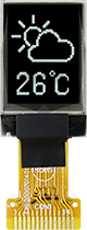
►Type: Graphique
►Structure: COG
►Dimension: 0.71 pouces
►Matrice de points 48 x 64
►Contrôleur intégré SSD1306
►Alimentation 3V
►1/64 duty
►Interface: I2C
►Couleur d'affichage: Blanc / Jaune / Bleu ciel
►Other FPC options available in below table
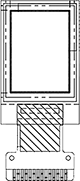
DESSIN
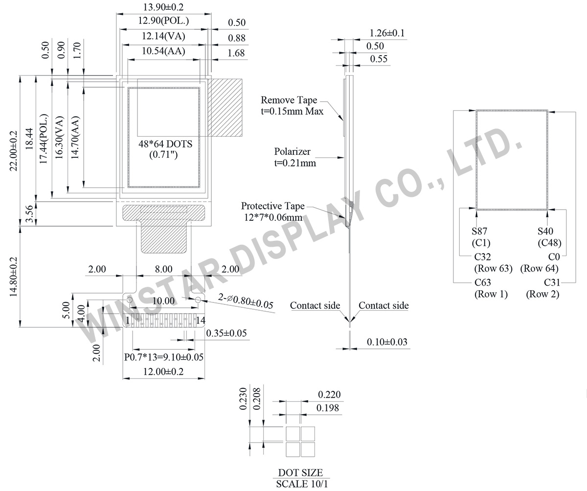
Data source ref: WEO004864AWPP3N00000
SPÉCIFICATIONS
Fonction PIN sur l'interface
| No. | Symbole | Function |
|---|---|---|
| 1 | C2N | Positive Terminal of the Flying Inverting Capacitorr Negative Terminal of the Flying Boost Capacitor The charge-pump capacitors are required between the terminals. They must be floated when the converter is not used. |
| 2 | C2P | |
| 3 | C1P | |
| 4 | C1N | |
| 5 | VBAT | Power Supply for DC/DC Converter Circuit This is the power supply pin for the internal buffer of the DC/DC voltage converter. It must be connected to external source when the converter is used. It should be connected to VDD when the converter is not used. |
| 6 | NC | No connection. |
| 7 | VSS | Ground of Logic Circuit This is a ground pin. It acts as a reference for the logic pins. It must be connected to external ground. |
| 8 | VDD | Power Supply for Logic This is a voltage supply pin. It must be connected to external source. |
| 9 | RES# | Power Reset for Controller and Driver This pin is reset signal input. When the pin is low, initialization of the chip is executed. |
| 10 | SCL | Host Data Input/Output Bus When serial mode is selected, D1 will be the serial data input SDIN and D0 will be the serial clock input SCLK. When I2C mode is selected, D2 & D1 should be tired together and serve as SDAout & SDAin in application and D0 is the serial clock input SCL. |
| 11 | SDA | |
| 12 | IREF | This is segment output current reference pin. When external IREF is used, a resistor should be connected between this pin and Vss to maintain the IREF current at a maximum of 30uA. When internal IREF is used, this pin should be kept NC |
| 13 | VCOMH | Voltage Output High Level for COM Signal This pin is the input pin for the voltage output high level for COM signals. A capacitor should be connected between this pin and VSS. |
| 14 | VCC | Power Supply for OEL Panel This is the most positive voltage supply pin of the chip. A stabilization capacitor should be connected between this pin and VSS when the converter is used. It must be connected to external source when the converter is not used. |
Données mécaniques
| Article | Dimensions | Unité |
|---|---|---|
| Matrice de points | 48 × 64 Dots | - |
| Module dimension | 13.90 × 22.0 × 1.26 | mm |
| Zone active | 10.54 × 14.70 | mm |
| Pixel Size | 0.198 × 0.208 | mm |
| Pixel Pitch | 0.220 × 0.230 | mm |
| Display Mode | Matrice passive | |
| Couleur d'affichage | Monochrome | |
| Drive Duty | 1/64 Duty | |
| IC | SSD1306 | |
| Interface | I2C | |
| Diagonale | 0.71 pouces | |
Valeurs nominales maximales absolues
| Parameter | Symbole | Min | Max | Unité |
|---|---|---|---|---|
| Supply Voltage for Logic | VDD | 0 | 4 | V |
| Supply Voltage for Display | VCC | 0 | 15 | V |
| Température de fonctionnement | TOP | -40 | +80 | °C |
| Température de stockage | TSTG | -40 | +85 | °C |
Caractéristiques électroniques
| Article | Symbole | État | Min | Typ | Max | Unité |
|---|---|---|---|---|---|---|
| Supply Voltage for Logic | VDD | - | 2.8 | 3 | 3.3 | V |
| Supply Voltage for Display | VCC | - | 7.0 | 7.5 | 8.0 | V |
| Input High Volt. | VIH | - | 0.8 xVDD | - | VDD | V |
| Input Low Volt. | VIL | - | 0 | - | 0.2 xVDD | V |
| Output High Volt. | VOH | - | 0.9 xVDD | - | VDD | V |
| Output Low Volt. | VOL | - | 0 | - | 0.1 xVDD | V |
| 50% Check Board operating Current | ICC | VCC=7.5V | - | 15 | 25.0 | mA |
FPC options
| Drawing | FPC Length | PIN | pitch | ZIF FPC or HOTBAR FPC | Interface | FPC No. | Create Date |
|---|---|---|---|---|---|---|---|
 |
16.0 | 14 | 0.7 | HOTBAR FPC | I2C | FPC2000701401XXXXX00 | 20160603 |
 |
11.2 | 14 | 0.7 | HOTBAR FPC | I2C | FPC2070001401XXXXX02 | 20180307 |
Search keyword: 48x64 oled, oled 48x64, 0.71 oled, 0.71 " oled, 0.71 inch oled, oled 0.71 , oled 0.71 "
