


Modello numero WF70A8SYAHLNT0
►Dimensione: 7 pollici
►Risoluzione : 1024x600 punti
►Direzione di visione : 85/85/85/85 (IPS)
►Interfaccia : LVDS
►TFT Driver IC : ST5021 + ST5651
►Scheda di controllo : No
►Luminosità (cd/m²): 800
►Cornice di fissaggio: No
►Touch Screen : con pannello touch resistivo (RTP)
DISEGNO
SPECIFICHE TECNICHE
Funzione dei Pin di Interfaccia
LCM PIN Definition
| Pin No. | Simbolo | I/O | Funzione |
|---|---|---|---|
| 1 | VCOM | P | Common Voltage |
| 2 | VDD | P | Digital circuit |
| 3 | VDD | P | Digital circuit |
| 4 | NC | --- | No connection |
| 5 | RESET | I | Global reset pin |
| 6 | STBYB | I | Standby mode, Normally pulled high STBYB = “1”, normal operation STBYB = “0”, timing controller, source driver will turn off, all output are High-Z |
| 7 | GND | P | Ground |
| 8 | RXIN0- | I | Negative LVDS differential data input |
| 9 | RXIN0+ | I | Positive LVDS differential data input |
| 10 | GND | P | Ground |
| 11 | RXIN1- | I | Negative LVDS differential data input |
| 12 | RXIN1+ | I | Positive LVDS differential data input |
| 13 | GND | P | Ground |
| 14 | RXIN2- | I | Negative LVDS differential data input |
| 15 | RXIN2+ | I | Positive LVDS differential data input |
| 16 | GND | P | Ground |
| 17 | RXCLKIN- | I | Negative LVDS differential clock input |
| 18 | RXCLKIN+ | I | Positive LVDS differential clock input |
| 19 | GND | P | Ground |
| 20 | RXIN3- | I | Negative LVDS differential data input |
| 21 | RXIN3+ | I | Positive LVDS differential data input |
| 22 | GND | P | Ground |
| 23 | NC | --- | No connection |
| 24 | NC | --- | No connection |
| 25 | GND | P | Ground |
| 26 | NC | --- | No connection |
| 27 | NC | --- | No connection |
| 28 | SELB | I | 6bit/8bit mode select H:6bit / L:8bit |
| 29 | AVDD | P | Power for Analog Circuit |
| 30 | GND | P | Ground |
| 31 | LED- | P | LED Cathode |
| 32 | LED- | P | LED Cathode |
| 33 | L/R | I | Horizontal inversion |
| 34 | U/D | I | Vertical inversion |
| 35 | VGL | P | Negative power for TFT |
| 36 | NC | --- | No connection |
| 37 | NC | --- | No connection |
| 38 | VGH | P | Positive power for TFT |
| 39 | LED+ | P | LED Anode |
| 40 | LED+ | P | LED Anode |
I:input ,O:output,P:power
Specifiche generali
| Articolo | Dimensioni | Unità |
|---|---|---|
| Dimensione (Diagonale) | 7 | pollici |
| A matrice di punti (Risoluzione) | 1024 × RGB × 600(TFT) | dots |
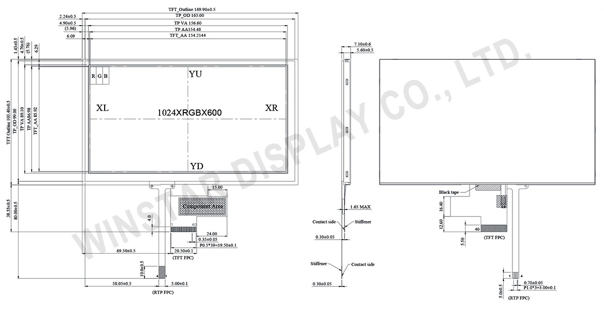
| Dimensione del modulo | 169.9(W) × 103.4(H) × 7.1(D) | mm |
| Area attiva | 154.2144 × 85.92 | mm |
| Passo del Dot | 0.1506 × 0.1432 | mm |
| LCD type | TFT, Nero, Trasmissivo | |
| Direzione di visione | 85/85/85/85 | |
| Proporzioni dell’area visiva (ratio) | 16:9 | |
| TFT Driver IC | ST5021 + ST5651 o equivalente | |
| Tipo di backlight | LED, Bianco | |
| Touch Panel | con pannello touch resistivo (RTP) | |
| TFT Interfaccia | LVDS | |
| Superficie | Anti-Glare | |
Valori massimi assoluti
| Articolo | Simbolo | Valore Min | Valore tipico | Valore massimo | Unità |
|---|---|---|---|---|---|
| Temperatura di lavoro | TOP | -20 | - | +70 | ℃ |
| Temperatura di stock | TST | -30 | - | +80 | ℃ |
Caratteristiche elettriche
| Articolo | Simbolo | Valore standard | Unità | ||
|---|---|---|---|---|---|
| Valore Min | Valore tipico | Valore massimo | |||
| Power voltage | VDD | 3.0 | 3.3 | 3.6 | V |
| Analog Power | AVDD | 8.9 | 9.0 | 9.1 | V |
| TFT Gate ON Voltage | VGH | 17 | 18 | 19 | V |
| TFT Gate OFF Voltage | VGL | -6.5 | -6.0 | -5.5 | V |
| TFT Common Voltage | Vcom | 3.0 | 3.15 | 3.3 | V |
| Current for Driver | IDD | - | 14 | 21 | mA |
| Power Current | IAVDD | - | 25 | - | mA |
| TFT Gate ON Current | IVGH | - | 1 | - | mA |
| TFT Gate OFF Current | IVGL | - | 1 | - | mA |
| TFT Common Current | IVCOM | - | 1 | - | mA |


