
")
")
")
")
")
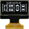
1.28インチ128x64 グラフィック液晶有機モジュール (ZIF FPC)
型番 WEO012864L-ZIF
►タイプ: グラフィック液晶有機
►結構: COG + ZIF FPC
►サイズ: 1.28インチ
►128x64 Dot Matrix
►3V電源
►1/64 duty cycle
►インターフェース: 6800 / 8080 / 3-SPI /4-SPI / I2C
►SH1106コントローラー内蔵
►発光色: 白色 / 黄色 / 空色
►Other FPC options available in below table
製品情報
外形図
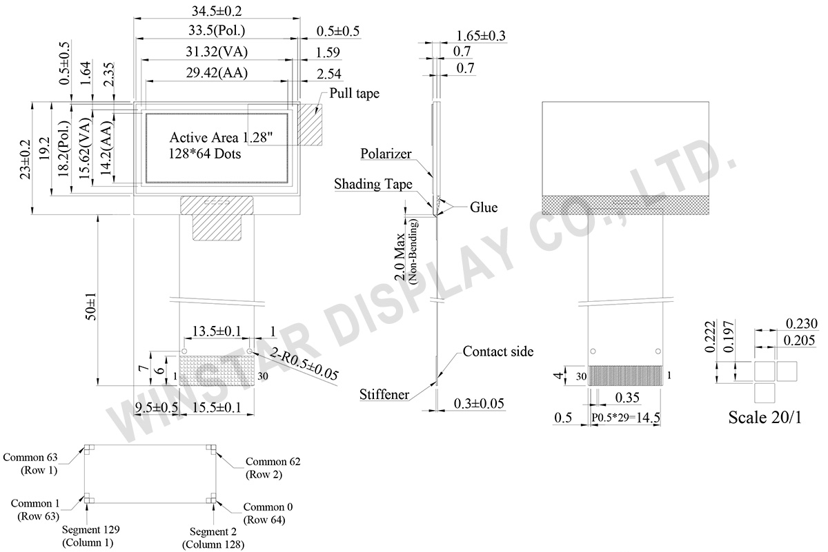
製品仕様
ピン功能定義
| No. | 記号 | 説明 | ||||||||||||||||||||||||
|---|---|---|---|---|---|---|---|---|---|---|---|---|---|---|---|---|---|---|---|---|---|---|---|---|---|---|
| 1 | NC(GND) | No connection | ||||||||||||||||||||||||
| 2 | C1N | Connect to charge pump capacitor. These pins are not used and should be disconnected when Vpp is supplied externally. |
||||||||||||||||||||||||
| 3 | C1P | |||||||||||||||||||||||||
| 4 | C2P | Connect to charge pump capacitor. These pins are not used and should be disconnected when Vpp is supplied externally. |
||||||||||||||||||||||||
| 5 | C2N | |||||||||||||||||||||||||
| 6 | VDD2 | 3.0 – 4.7V power supply pad for Power supply for charge pump circuit. This pin should be disconnected when VPP is supplied externally |
||||||||||||||||||||||||
| 7 | NC | No connection | ||||||||||||||||||||||||
| 8 | VSS | Ground. | ||||||||||||||||||||||||
| 9 | VDD1 | Power supply input: 1.65 - 3.5V | ||||||||||||||||||||||||
| 10 | IM0 | These are the MPU interface mode select pads.
|
||||||||||||||||||||||||
| 11 | IM1 | |||||||||||||||||||||||||
| 12 | IM2 | |||||||||||||||||||||||||
| 13 | CSB | This pad is the chip select input. When CSB = “L”, then the chip select becomes active, and data/command I/O is enabled. | ||||||||||||||||||||||||
| 14 | RESB | This is a reset signal input pad. When RES is set to “L”, the settings are initialized. The reset operation is performed by the RES signal level. | ||||||||||||||||||||||||
| 15 | A0 | This is the Data/Command control pad that determines whether the data bits are data or a command. A0 = “H”: the inputs at D0 to D7 are treated as display data. A0 = “L”: the inputs at D0 to D7 are transferred to the command registers. In I2C interface, this pad serves as SA0 to distinguish the different address of OLED driver. |
||||||||||||||||||||||||
| 16 | WRB | This is a MPU interface input pad. When connected to an 8080 MPU, this is active LOW. This pad connects to the 8080 MPU WR signal. The signals on the data bus are latched at the rising edge of the WR signal. When connected to a 6800 Series MPU: This is the read/write control signal input terminal. When R/W = “H”: Read. When R/W = “L”: Write. |
||||||||||||||||||||||||
| 17 | RDB | This is a MPU interface input pad. When connected to an 8080 series MPU, it is active LOW. This pad is connected to the RD signal of the 8080 series MPU, and the data bus is in an output status when this signal is “L”. When connected to a 6800 series MPU , this is active HIGH. This is used as an enable clock input of the 6800 series MPU. When RD = “H”: Enable. When RD = “L”: Disable. |
||||||||||||||||||||||||
| 18 | D0 | This is an 8-bit bi-directional data bus that connects to an 8-bit or 16-bit standard MPU data bus. When the serial interface is selected, then D0 serves as the serial clock input pad (SCL) and D1 serves as the serial data input pad (SI). At this time, D2 to D7 are set to high impedance. When the I2C interface is selected, then D0 serves as the serial clock input pad (SCL) and D1 serves as the serial data input pad (SDAI). At this time, D2 to D7 are set to high impedance. |
||||||||||||||||||||||||
| 19 | D1 | |||||||||||||||||||||||||
| 20 | D2 | |||||||||||||||||||||||||
| 21 | D3 | |||||||||||||||||||||||||
| 22 | D4 | |||||||||||||||||||||||||
| 23 | D5 | |||||||||||||||||||||||||
| 24 | D6 | |||||||||||||||||||||||||
| 25 | D7 | |||||||||||||||||||||||||
| 26 | IREF | This is a segment current reference pad. A resistor should be connected between this pad and VSS. Set the current at 18.75uA. | ||||||||||||||||||||||||
| 27 | VCOMH | This is a pad for the voltage output high level for common signals. A capacitor should be connected between this pad and VSS. |
||||||||||||||||||||||||
| 28 | VPP | OLED panel power supply. Generated by internal charge pump. Connect to capacitor. It could be supplied externally. |
||||||||||||||||||||||||
| 29 | VSL | This is a segment voltage reference pad. This pad should be connected to VSS externally. |
||||||||||||||||||||||||
| 30 | NC(GND) | No connection |
規格説明
| 項目 | 標準値 | 単位 |
|---|---|---|
| ドットマトリックス(解像度) | 128 x 64 | - |
| 外形寸法 | 34.50 × 23.00 × 1.65 | mm |
| 有効表示エリア | 29.42 × 14.20 | mm |
| ドットサイズ | 0.205 × 0.197 | mm |
| ドットピッチ | 0.230 × 0.222 | mm |
| 表示モード | パッシブマトリクス | |
| 発光色 | Monochrome | |
| 駆動方法 | 1/64 Duty | |
| コントローラー IC | SH1106 | |
| インターフェイス | 6800/8080/3-SPI /4-SPI / I2C | |
| サイズ | 1.28 インチ | |
絶対最大定格
| パラメーター | 記号 | 最小値 | 最大値 | 単位 |
|---|---|---|---|---|
| ロジック電源電圧 | VDD1 | -0.3 | 3.6 | V |
| Power supply for charge pump circuit | VDD2 | -0.3 | 4.8 | V |
| Display電源電圧 | VPP | -0.3 | 14.5 | V |
| 操作温度 | TOP | -40 | +80 | °C |
| 保存温度 | TSTG | -40 | +85 | °C |
電気特性
DC電気特性
| 項目 | 記号 | 条件 | 最小値 | 典型値 | 最大値 | 単位 |
|---|---|---|---|---|---|---|
| ロジック電源電圧 | VDD1 | - | 2.8 | 3.0 | 3.3 | V |
| Display電源電圧 | VPP | - | 6.75 | 7.25 | 7.75 | V |
| 高レベル入力 | VIH | - | 0.8xVDD1 | - | VDD1 | V |
| 低レベル入力 | VIL | - | VSS | - | 0.2xVDD1 | V |
| 高レベル出力 | VOH | - | 0.8xVDD1 | - | VDD1 | V |
| 低レベル出力 | VOL | - | VSS | - | 0.2xVDD1 | V |
| 50% Check Board operating Current | VPP =7.25V | 5.0 | 6.0 | 7.0 | mA | |
FPC options
| Drawing | FPC Length | PIN | Pitch | ZIF FPC or HOTBAR FPC | Interface | FPC No. | Create Date |
|---|---|---|---|---|---|---|---|
 |
13.2 | 30 | 0.7 | HOTBAR FPC | 6800/8080/3-SPI /4-SPI / I2C | FPC2070003001XXXXX03 | 20141107 |
 |
51.15 | 30 | 0.5 | ZIF | 6800/8080/3-SPI /4-SPI / I2C | FPC2050003011XXXXX18 | 20180123 |
Search keyword: 128x64 oled, oled 128x64, 1.28 oled, 1.28" oled, 1.28 インチ oled, oled 1.28, oled 1.28"
