


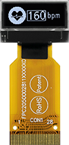
96x32 Graficzne OLED 0.68 cale (ZIF FPC)
Numer modelu WEO009632B-ZIF
►Typ: graficzny
►Struktura: COG + ZIF FPC
►Rozmiar: 0.68"
►96 x 32 matryca punktowa
►wbudowany kontroler SSD1305
►zasilanie 3V
►wypełnienie 1/32
►interfejs: 6800, 8080, SPI, I2C
►Kolor wyświetlacza: biały / żółto
►Other FPC options available in below table
Opis
Rysunek
Data source ref: WEO009632BLAP3N00000
Specyfikacja
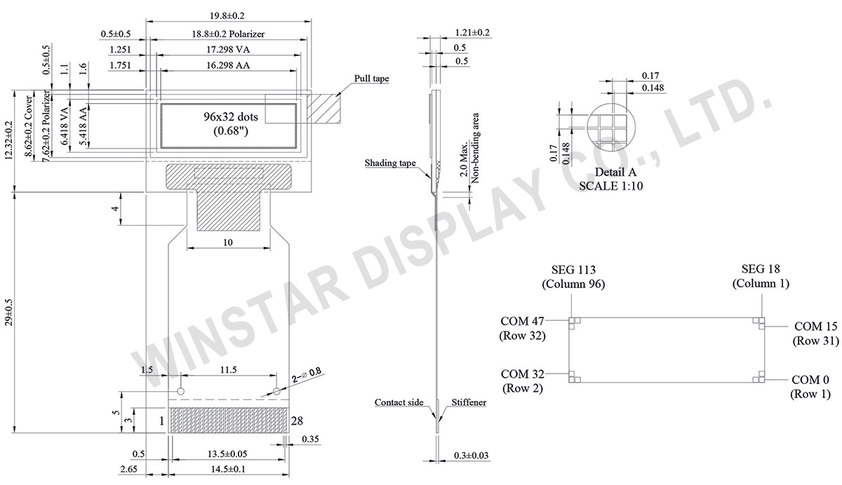
Funkcja pinów interfejsu
| Pin | Symbol | I/O | Funkcja | |||||||||||||||
|---|---|---|---|---|---|---|---|---|---|---|---|---|---|---|---|---|---|---|
| 1 | VSS | - | Reserved Pin(Supporting Pin) The supporting pins can reduce the influences from stresses on the function pins. These pins must be connected to external ground. |
|||||||||||||||
| 2 | GDR | - | Reserved pin, not connected. | |||||||||||||||
| 3 | VDDB | P | Reserved pin, not connected. | |||||||||||||||
| 4 | FB | - | Reserved pin, not connected. | |||||||||||||||
| 5 | NC | - | Not connected. | |||||||||||||||
| 6 | VBREF | - | Reserved pin, not connected. | |||||||||||||||
| 7 | NC | - | Not connected. | |||||||||||||||
| 8 | NC | - | Not connected. | |||||||||||||||
| 9 | VDD | P | Power supply pin for core logic operation. | |||||||||||||||
| 10 | BS1 | I | MCU bus interface selection pins. Select appropriate logic setting as described in the following table. BS2, and BS1 are pin select.
|
|||||||||||||||
| 11 | BS2 | I | ||||||||||||||||
| 12 | NC | - | Not connected. | |||||||||||||||
| 13 | CS# | I | This pin is the chip select input connecting to the MCU. The chip is enabled for MCU communication only when CS# is pulled LOW (active LOW). |
|||||||||||||||
| 14 | RES# | I | This pin is reset signal input. When the pin is pulled LOW, initialization of the chip is executed. Keep this pin HIGH (i.e. connect to VDD) during normal operation. | |||||||||||||||
| 15 | D/C# | I | This pin is Data/Command control pin connecting to the MCU. When the pin is pulled HIGH, the data at D[7:0] will be interpreted as data. When the pin is pulled LOW, the data at D[7:0] will be transferred to a command register. In I2C mode, this pin acts as SA0 for slave address selection. |
|||||||||||||||
| 16 | WR# | I | This is read / write control input pin connecting to the MCU interface. When interfacing to a 6800-series microprocessor, this pin will be used as Read/Write (R/W#) selection input. Read mode will be carried out when this pin is pulled HIGH (i.e. connect to VDD) and write mode when LOW. When 8080 interface mode is selected, this pin will be the Write (WR#) input. Data write operation is initiated when this pin is pulled LOW and the chip is selected. When serial or I2C interface is selected, this pin must be connected to VSS. |
|||||||||||||||
| 17 | E/RD# | I | This pin is MCU interface input. When 6800 interface mode is selected, this pin will be used as the Enable (E) signal. Read/write operation is initiated when this pin is pulled HIGH and the chip is selected. When 8080 interface mode is selected, this pin receives the Read (RD#) signal. Read operation is initiated when this pin is pulled LOW and the chip is selected. When serial or I2C interface is selected, this pin must be connected to VSS. |
|||||||||||||||
| 18~25 | D0~D7 | - | These are 8-bit bi-directional data bus to be connected to the microprocessor’s data bus. When serial interface mode is selected, D0 will be the serial clock input: SCLK; D1 will be the serial data input: SDIN. When I2C mode is selected, D2, D1 should be tied together and serve as SDAout, SDAin in application and D0 is the serial clock input, SCL. |
|||||||||||||||
| 26 | IREF | - | This is segment output current reference pin. When external IREF is used, a resistor should be connected between this pin and VSS to maintain the IREF current at 30uA. |
|||||||||||||||
| 27 | VCOMH | - | COM signal deselected voltage level. A capacitor should be connected between this pin and VSS. |
|||||||||||||||
| 28 | VCC | - | Power supply for panel driving voltage. This is also the most positive power voltage supply pin. When charge pump is enabled, a capacitor should be connected between this pin and VSS. |
Dane mechaniczne
| Rzecz | Wymiar | Jednostka |
|---|---|---|
| Rozdzielczość | 96 × 32 | pikseli |
| Wymiary modułu | 19.80 × 12.32 × 1.21 (mm) | mm |
| Obszar aktywny | 16.298 × 5.418 (mm) | mm |
| Wielkość piksela | 0.148 × 0.148 (mm) | mm |
| Raster pomiędzy pikselami | 0.17 × 0.17 (mm) | mm |
| Tryb wyświetlania | matryca | |
| Kolor wyświetlacza | Monochromatyczny | |
| Drive Duty | 1/32 Duty | |
| IC | SSD1305 | |
| Interfejs | 6800, 8080, SPI, I2C | |
| Przekątna | 0.68 calowy | |
Bezwzględne oceny maksymalne
| Parameter | Symbol | Minimalna wartość | Maksymalna wartość | Jednostka |
|---|---|---|---|---|
| Supply Voltage for Logic | VDD | -0.3 | 4 | V |
| Supply Voltage for Display | VCC | 0 | 16 | V |
| Temperatura pracy | TOP | -40 | +80 | °C |
| Temperatura przechowywania | TSTG | -40 | +85 | °C |
Parametry elektryczne
DC elektryczne
| Rzecz | Symbol | Stan | Minimalna wartość | Typowa wartość | Maksymalna wartość | Jednostka |
|---|---|---|---|---|---|---|
| Supply Voltage for Logic | VDD | - | 2.8 | 3.0 | 3.3 | V |
| Supply Voltage for Display | VCC | - | 11.5 | 12 | 12.5 | V |
| High Level Input | VIH | - | 0.8×VDD | - | VDD | V |
| Low Level Input | VIL | - | 0 | - | 0.2×VDD | V |
| High Level Output | VOH | Iout = 100uA | 0.9×VDD | - | VDD | V |
| Low Level Output | VOL | Iout = 100uA | 0 | - | 0.1×VDD | V |
| Symbol | Parameter | Minimalna wartość | Typowa wartość | Maksymalna wartość | Jednostka | Stan |
|---|---|---|---|---|---|---|
| ICC | VCC Supply Current | - | 5.0 | 7.5 | mA | VDD =3.0V , Display 100% ON |
FPC options
| Drawing | FPC Length | PIN | pitch | ZIF FPC or HOTBAR FPC | Interface | FPC No. | Create Date |
|---|---|---|---|---|---|---|---|
 |
30 | 28 | 0.5 | ZIF FPC | 6800, 8080,4-Wire SPI, I2C | FPC2050002811XXXXX01 | 20180131 |
 |
8.479 | 25 | 0.65 | HOTBAR FPC | 6800, 8080,4-Wire SPI, I2C | FPC2065002501XXXXX00 | 20190906 |
Search keyword: 96x32 oled, oled 96x32, 0.68 oled, 0.68" oled, 0.68 calowy oled, oled 0.68"
