

0.96" 128x64 SSD1315 OLED Ekran
Model No. WEO012864V
►Türü : Grafik
►Yapı : COG
►Boyut : 0.96 inç
►128 x 64 dot matrisi
►Kontrolör dahil SSD1315
►3V güç sağlayıcı
►1/64 görev
►Ara yüz : SPI, I2C
►OLED Rengi: Beyaz
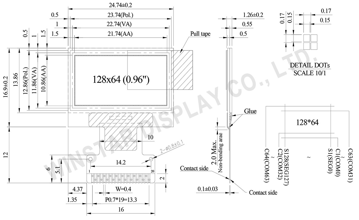
ÇIZIM
Data source ref: WEO012864VWPP3N0Y000
AYRINTILAR
Arayüz Pin Fonksiyonlari
| No. | Sembol | Fonksiyon | ||||||||
|---|---|---|---|---|---|---|---|---|---|---|
| 1 | C2N | C2P/C2N – Pin for charge pump capacitor; Connect to each other with a capacitor. | ||||||||
| 2 | C2P | |||||||||
| 3 | C1P | C1P/C1N – Pin for charge pump capacitor; Connect to each other with a capacitor. | ||||||||
| 4 | C1N | |||||||||
| 5 | VBAT | Power Supply for DC/DC Converter Circuit This is the power supply pin for the internal buffer of the DC/DC voltage converter. It must be connected to external source when the converter is used. It should be float when the converter is not used. |
||||||||
| 6 | VCC | Power supply for panel driving voltage. This is also the most positive power voltage supply pin. When charge pump is enabled, a capacitor should be connected between this pin and VSS. |
||||||||
| 7 | VSS | Ground of Logic Circuit This is a ground pin. It acts as a reference for the logic pins. It must be connected to external ground. |
||||||||
| 8 | VDD | Power Supply for Logic This is a voltage supply pin. It must be connected to external source. |
||||||||
| 9 | BS0 | Communicating Protocol Select These pins are MCU interface selection input. See the following table:
|
||||||||
| 10 | BS1 | |||||||||
| 11 | CS# | Chip Select This pin is the chip select input. The chip is enabled for MCU communication only when CS# is pulled low. |
||||||||
| 12 | RES# | Power Reset for Controller and Driver This pin is reset signal input. When the pin is low, initialization of the chip is executed. |
||||||||
| 13 | D/C# | In I2C mode, this pin acts as SA0 for slave address selection. When 3-wire serial interface is selected, this pin must be connected to VSS. |
||||||||
| 14~16 | D0~D2 | When serial interface mode is selected, D0 will be the serial clock input: SCLK; D1 will be the serial data input: SDIN. When I2C mode is selected, D2, D1 should be tied together and serve as SDAout, SDAin in application and D0 is the serial clock input, SCL. |
||||||||
| 17 | IREF | Current Reference for Brightness Adjustment This pin is segment current reference pin. A resistor should be connected between this pin and VSS. Set the current lower than 30uA. |
||||||||
| 18 | VCOMH | COM signal deselected voltage level. A capacitor should be connected between this pin and VSS. |
||||||||
| 19 | VCC | Power supply for panel driving voltage. This is also the most positive power voltage supply pin. When charge pump is enabled, a capacitor should be connected between this pin and VSS. |
||||||||
| 20 | VLSS | Ground of Analog Circuit This is an analog ground pin. It should be connected to VSS externally. |
Mekanik Veri
| Kalem | Ölçü | Birim |
|---|---|---|
| Nokta Matrisi | 128 x 64 Dots | - |
| Modül ölçüleri | 24.74 x 16.90 x 1.26 | mm |
| Aktif alan | 21.74 x 10.86 | mm |
| Nokta boyutu | 0.15 x 0.15 | mm |
| Nokta sıklığı | 0.17 x 0.17 | mm |
| Display Mode | Pasif Matrisli | |
| Display Color | Monochrome | |
| Drive Duty | 1/64 Duty | |
| IC | SSD1315 | |
| Arayüz | 4-line/3-line SPI, I2C | |
| Boyut | 0.96 inç | |
Maksimum Değerler
| Parameter | Symbol | Minumum Deger | Maksimum Deger | Birim |
|---|---|---|---|---|
| Supply Voltage for Logic | VDD | -0.3 | 4.0 | V |
| Charge Pump Regulator | VBAT | -0.3 | 6.0 | V |
| Supply Voltage for Display | VCC | 0 | 18.0 | V |
| Çalışma Sıcaklığı | TOP | -30 | +70 | °C |
| Saklama Sıcaklığı | TSTG | -30 | +70 | °C |
Elektronik Özellikleri
DC Elektronik Özellikleri
| Kalem | Sembol | Durum | Minumum Deger | Tipik Deger | Maksimum Deger | Birim |
|---|---|---|---|---|---|---|
| Supply Voltage for Logic | VDD | - | 2.8 | 3.0 | 3.3 | V |
| Supply Voltage for Display | VCC | - | 7.0 | 7.5 | 8.0 | V |
| Input High Volt. | VIH | - | 0.8×VDD | - | VDD | V |
| Input Low Volt. | VIL | - | 0 | - | 0.2×VDD | V |
| Output High Volt. | VOH | - | 0.9×VDD | - | VDD | V |
| Output Low Volt. | VOL | - | 0 | - | 0.1×VDD | V |
| Operating Current for VCC (50% display ON) | ICC | - | - | 6 | 12 | mA |
Search keyword: 128x64 oled, oled 128x64, 0.96 oled, 0.96" oled, 0.96 inç oled, oled 0.96, oled 0.96"


