N° de modèle WF70A8TYAHLNN0
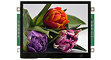
►Dimension 7 pouces
►Résolution d’écran: 1024x600 points
►Vue préférentielle 85/85/85/85 (IPS)
►Interface: LVDS
►TFT CI pilote: ST5021 + ST5651
►Carte de contrôle: NON
►Luminosité (Cd/m²): 600
►cadre de maintien avec points de fixation: NON
►Dalle tactile: NON
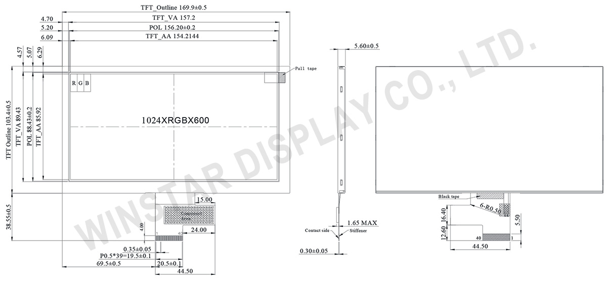
DESSIN
SPÉCIFICATIONS
Fonction PIN sur l'interface
LCM PIN Definition
| Pin No. | Symbole | I/O | Function |
|---|---|---|---|
| 1 | VCOM | P | Common Voltage |
| 2 | VDD | P | Digital circuit |
| 3 | VDD | P | Digital circuit |
| 4 | NC | --- | No connection |
| 5 | RESET | I | Global reset pin |
| 6 | STBYB | I | Standby mode, Normally pulled high STBYB = “1”, normal operation STBYB = “0”, timing controller, source driver will turn off, all output are High-Z |
| 7 | GND | P | Ground |
| 8 | RXIN0- | I | Negative LVDS differential data input |
| 9 | RXIN0+ | I | Positive LVDS differential data input |
| 10 | GND | P | Ground |
| 11 | RXIN1- | I | Negative LVDS differential data input |
| 12 | RXIN1+ | I | Positive LVDS differential data input |
| 13 | GND | P | Ground |
| 14 | RXIN2- | I | Negative LVDS differential data input |
| 15 | RXIN2+ | I | Positive LVDS differential data input |
| 16 | GND | P | Ground |
| 17 | RXCLKIN- | I | Negative LVDS differential clock input |
| 18 | RXCLKIN+ | I | Positive LVDS differential clock input |
| 19 | GND | P | Ground |
| 20 | RXIN3- | I | Negative LVDS differential data input |
| 21 | RXIN3+ | I | Positive LVDS differential data input |
| 22 | GND | P | Ground |
| 23 | NC | --- | No connection |
| 24 | NC | --- | No connection |
| 25 | GND | P | Ground |
| 26 | NC | --- | No connection |
| 27 | NC | --- | No connection |
| 28 | SELB | I | 6bit/8bit mode select H:6bit / L:8bit |
| 29 | AVDD | P | Power for Analog Circuit |
| 30 | GND | P | Ground |
| 31 | LED- | P | LED Cathode |
| 32 | LED- | P | LED Cathode |
| 33 | L/R | I | Horizontal inversion |
| 34 | U/D | I | Vertical inversion |
| 35 | VGL | P | Negative power for TFT |
| 36 | NC | --- | No connection |
| 37 | NC | --- | No connection |
| 38 | VGH | P | Positive power for TFT |
| 39 | LED+ | P | LED Anode |
| 40 | LED+ | P | LED Anode |
I:input ,O:output,P:power
Spécifications générales
| Article | Dimensions | Unité |
|---|---|---|
| Diagonale | 7 | pouces |
| Matrice de points (Résolution) | 1024 × RGB × 600(TFT) | points |
| Dimensions du module | 169.9(W) × 103.4(H) × 5.6(D) | mm |
| Zone active | 154.2144 × 85.92 | mm |
| Pas des points | 0.1506 × 0.1432 | mm |
| Type de LCD | TFT, Noir, Transmissif | |
| Vue préférentielle | 85/85/85/85 | |
| Rapport d'aspect | 16:9 | |
| TFT CI pilote | ST5021 + ST5651 ou équivalent | |
| Type de rétroéclairage | LED, Blanc | |
| Dalle tactile | Sans dalle tactile | |
| TFT Interface | LVDS | |
| Surface | Anti-reflets | |
Valeurs nominales maximales absolues
| Article | Symbole | Valeur min | Valeur type | Valeur max | Unité |
|---|---|---|---|---|---|
| Température de fonctionnement | TOP | -20 | - | +70 | ℃ |
| Température de stockage | TST | -30 | - | +80 | ℃ |
Caractéristiques électroniques
| Article | Symbole | Valeur standard | Unité | ||
|---|---|---|---|---|---|
| Valeur min | Valeur type | Valeur max | |||
| Power voltage | VDD | 3.0 | 3.3 | 3.6 | V |
| Analog Power | AVDD | 8.9 | 9.0 | 9.1 | V |
| TFT Gate ON Voltage | VGH | 17 | 18 | 19 | V |
| TFT Gate OFF Voltage | VGL | -6.5 | -6.0 | -5.5 | V |
| TFT Common Voltage | Vcom | 3.0 | 3.15 | 3.3 | V |
| Current for Driver | IDD | - | 14 | 21 | mA |
| Power Current | IAVDD | - | 25 | - | mA |
| TFT Gate ON Current | IVGH | - | 1 | - | mA |
| TFT Gate OFF Current | IVGL | - | 1 | - | mA |
| TFT Common Current | IVCOM | - | 1 | - | mA |