OLED Grafici 1.71"
Modello numero WEO012832G
►Tipo: grafico
►Struttura: COG
►Dimensione: 1.71 pollici
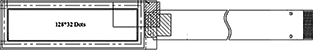
►128 x 32 a matrice di punti
►A bordo Controllore SSD1307
►Alimentatore 3V
►1/32 duty
►Interfaccia: SPI, I2C
►Colore display: Bianco / Giallo
►Other FPC options available in below table
DESCRIZIONE
DISEGNO
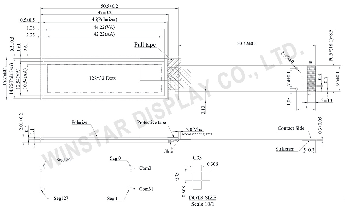
Data source ref: WEO012832GWAP3N00000
SPECIFICHE TECNICHE
Funzione dei Pin di Interfaccia
| No. | Simbolo | Funzione | ||||||||||||
|---|---|---|---|---|---|---|---|---|---|---|---|---|---|---|
| 1 | N.C. (GND) | Reserved Pin (Supporting Pin) The supporting pins can reduce the influences from stresses on the function pins. These pins must be connected to external ground. |
||||||||||||
| 2 | VCC | Power Supply for OEL Panel This is the most positive voltage supply pin of the chip. A stabilization capacitor should be connected between this pin and VSS when the converter is used. It must be connected to external source when the converter is not used. |
||||||||||||
| 3 | VLSS | Ground of Analog Circuit This is an analog ground pin. It should be connected to VSS externally. |
||||||||||||
| 4 | VSS | Ground of Logic Circuit This is a ground pin. It acts as a reference for the logic pins. It must be connected to external ground. |
||||||||||||
| 5 | VDD | Power Supply for Logic This is a voltage supply pin. It must be connected to external source. |
||||||||||||
| 6 | CS# | Chip Select This pin is the chip select input. The chip is enabled for MCU communication only when CS# is pulled low. |
||||||||||||
| 7 | RES# | Power Reset for Controller and Driver This pin is reset signal input. When the pin is low, initialization of the chip is executed. |
||||||||||||
| 8 | D/C# | Data/Command Control When the pin is pulled high and serial interface mode is selected, the data at SDIN is treated as data. When it is pulled low, the data at SDIN will be transferred to the command register. In I2C mode, this pin acts as SA0 for slave address selection. |
||||||||||||
| 9~11 | D0~D2 | Host Data Input/Output Bus When serial interface mode is selected, D0 will be the serial clock input: SCLK; D1 will be the serial data input: SDIN. When I2C mode is selected, D2, D1 should be tied together and serve as SDAout, SDAin in application and D0 is the serial clock input, SCL. |
||||||||||||
| 12 | IREF | Current Reference for Brightness Adjustment This pin is segment current reference pin. A resistor should be connected between this pin and VSS. Set the current lower than 12.5μA. |
||||||||||||
| 13 | VCOMH | Voltage Output High Level for COM Signal This pin is the input pin for the voltage output high level for COM signals. A capacitor should be connected between this pin and VSS. |
||||||||||||
| 14 | VCC | Power Supply for OEL Panel This is the most positive voltage supply pin of the chip. A stabilization capacitor should be connected between this pin and VSS when the converter is used. It must be connected to external source when the converter is not used. |
||||||||||||
| 15,16 | BS0 | Communicating Protocol Select These pins are MCU interface selection input. See the following table:
|
||||||||||||
| BS1 | ||||||||||||||
| 17 | VLSS | Ground of Analog Circuit This is an analog ground pin. It should be connected to VSS externally. |
||||||||||||
| 18 | N.C. (GND) | Reserved Pin (Supporting Pin) The supporting pins can reduce the influences from stresses on the function pins. These pins must be connected to external ground. |
Dati meccanici
| Articolo | Dimensioni | Unità |
|---|---|---|
| A matrice di punti | 128 × 32 | Dots |
| Dimensione del modulo | 50.50 × 15.75 × 2.01 | mm |
| Area attiva | 42.22 × 10.54 | mm |
| Dimensioni del Dot | 0.308 × 0.308 | mm |
| Passo del Dot | 0.33 × 0.33 | mm |
| Modalità display | Matrice passiva | |
| Colore display | Monocromatici | |
| Drive Duty | 1/32 Duty | |
| IC | SSD1307 | |
| Interfaccia | SPI, I2C | |
| Dimensione | 1.71 pollici | |
Caratteristiche elettriche
| Articolo | Simbolo | Condizione | Valore Min | Valore tipico | Valore massimo | Unità |
|---|---|---|---|---|---|---|
| Supply Voltage for Logic | VDD | - | 2.8 | 3.0 | 3.3 | V |
| Supply Voltage for Display | VCC | - | 11.5 | 12.0 | 12.5 | V |
| High Level Input | VIH | - | 0.8×VDD | - | - | V |
| Low Level Input | VIL | - | 0 | - | 0.2×VDD | V |
| High Level Output | VOH | - | 0.9×VDD | - | - | V |
| Low Level Output | VOL | - | - | - | 0.1×VDD | V |
| Operating Current for VCC (Full ON) | ICC | VCC=12.0V | - | 14.5 | 19.0 | mA |
Valori massimi assoluti
| Parameter | Simbolo | Valore Min | Valore massimo | Unità |
|---|---|---|---|---|
| Supply Voltage for Logic | VDD | -0.3 | 4.0 | V |
| Supply Voltage for Display | VCC | 0 | 16.0 | V |
| Operating Temperature | TOP | -40 | +80 | °C |
| Storage Temperature | TSTG | -40 | +85 | °C |
FPC options
| Drawing | FPC Length | PIN | Pitch | ZIF FPC or HOTBAR FPC | Interface | FPC No. | Create Date |
|---|---|---|---|---|---|---|---|
 |
51.5 | 18 | 0.5 | ZIF | SPI,I2C | FPC2050001811XXXXX01 | 20170607 |
 |
121.08 | 18 | 0.5 | ZIF | SPI,I2C | FPC2050001811XXXXX05 | 20181030 |
Search keyword: 128x32 oled, oled 128x32, 1.71 oled, 1.71" oled, 1.71 pollici oled, oled 1.71, oled 1.71"