


產品敘述
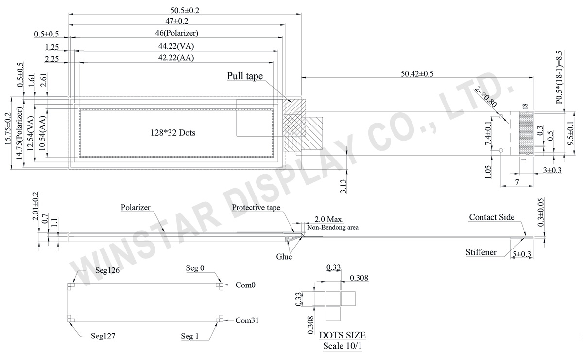
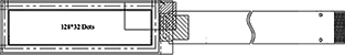
WEO012832G是一款1.71吋的PM OLED顯示器模組,解析度128x32 pixels。此款模組內建SSD1307 IC,模組支援 I2C與4-線SPI介面,3V電源供應,1/32 duty驅動。
1.71” 的WEO012832G是COG結構的OLED顯示器,無需背光非常輕薄,適用於智能家電產品、攜帶型裝置、智慧醫療產品、量測儀器等產品。此模組的工作溫度是-40℃至+80℃,儲存溫度-40℃至+85℃。
規格圖
Data source ref: WEO012832GWAP3N00000
產品規格
Pin功能定義
| No. | 符號 | 功能說明 | ||||||||||||
|---|---|---|---|---|---|---|---|---|---|---|---|---|---|---|
| 1 | N.C. (GND) | Reserved Pin (Supporting Pin) The supporting pins can reduce the influences from stresses on the function pins. These pins must be connected to external ground. |
||||||||||||
| 2 | VCC | Power Supply for OEL Panel This is the most positive voltage supply pin of the chip. A stabilization capacitor should be connected between this pin and VSS when the converter is used. It must be connected to external source when the converter is not used. |
||||||||||||
| 3 | VLSS | Ground of Analog Circuit This is an analog ground pin. It should be connected to VSS externally. |
||||||||||||
| 4 | VSS | Ground of Logic Circuit This is a ground pin. It acts as a reference for the logic pins. It must be connected to external ground. |
||||||||||||
| 5 | VDD | Power Supply for Logic This is a voltage supply pin. It must be connected to external source. |
||||||||||||
| 6 | CS# | Chip Select This pin is the chip select input. The chip is enabled for MCU communication only when CS# is pulled low. |
||||||||||||
| 7 | RES# | Power Reset for Controller and Driver This pin is reset signal input. When the pin is low, initialization of the chip is executed. |
||||||||||||
| 8 | D/C# | Data/Command Control When the pin is pulled high and serial interface mode is selected, the data at SDIN is treated as data. When it is pulled low, the data at SDIN will be transferred to the command register. In I2C mode, this pin acts as SA0 for slave address selection. |
||||||||||||
| 9~11 | D0~D2 | Host Data Input/Output Bus When serial interface mode is selected, D0 will be the serial clock input: SCLK; D1 will be the serial data input: SDIN. When I2C mode is selected, D2, D1 should be tied together and serve as SDAout, SDAin in application and D0 is the serial clock input, SCL. |
||||||||||||
| 12 | IREF | Current Reference for Brightness Adjustment This pin is segment current reference pin. A resistor should be connected between this pin and VSS. Set the current lower than 12.5μA. |
||||||||||||
| 13 | VCOMH | Voltage Output High Level for COM Signal This pin is the input pin for the voltage output high level for COM signals. A capacitor should be connected between this pin and VSS. |
||||||||||||
| 14 | VCC | Power Supply for OEL Panel This is the most positive voltage supply pin of the chip. A stabilization capacitor should be connected between this pin and VSS when the converter is used. It must be connected to external source when the converter is not used. |
||||||||||||
| 15,16 | BS0 | Communicating Protocol Select These pins are MCU interface selection input. See the following table:
|
||||||||||||
| BS1 | ||||||||||||||
| 17 | VLSS | Ground of Analog Circuit This is an analog ground pin. It should be connected to VSS externally. |
||||||||||||
| 18 | N.C. (GND) | Reserved Pin (Supporting Pin) The supporting pins can reduce the influences from stresses on the function pins. These pins must be connected to external ground. |
規格說明
| 項目 | 尺寸 | 單位 |
|---|---|---|
| 解析度 | 128 × 32 | Dots |
| 模組尺寸 | 50.50 × 15.75 × 2.01 | mm |
| 檢視區域 | 42.22 × 10.54 | mm |
| 點大小 | 0.308 × 0.308 | mm |
| 點間距 | 0.33 × 0.33 | mm |
| 顯示模式 | 被動矩陣 | |
| 發光顏色 | 單色 | |
| 驅動方式 | 1/32 Duty | |
| IC | SSD1307 | |
| 介面 | SPI,I2C | |
| 尺寸 | 1.71 吋 | |
電氣特性
| 項目 | 符號 | 條件 | 最小值 | 標準值 | 最大值 | 單位 |
|---|---|---|---|---|---|---|
| 邏輯電源電壓 | VDD | - | 2.8 | 3.0 | 3.3 | V |
| 顯示電源電壓 | VCC | - | 11.5 | 12.0 | 12.5 | V |
| 輸入高準位 | VIH | - | 0.8×VDD | - | - | V |
| 輸入低準位 | VIL | - | 0 | - | 0.2×VDD | V |
| 輸出高準位 | VOH | - | 0.9×VDD | - | - | V |
| 輸出低準位 | VOL | - | - | - | 0.1×VDD | V |
| VCC (Full ON) 工作電流 | ICC | VCC=12.0V | - | 14.5 | 19.0 | mA |
最大絕對額定值
| 參數 | 符號 | 最小值 | 最大值 | 單位 |
|---|---|---|---|---|
| 邏輯電源電壓 | VDD | -0.3 | 4.0 | V |
| 顯示電源電壓 | VCC | 0 | 16.0 | V |
| 工作溫度 | TOP | -40 | +80 | °C |
| 儲存溫度 | TSTG | -40 | +85 | °C |
FPC options
| Drawing | FPC Length | PIN | Pitch | ZIF FPC or HOTBAR FPC | Interface | FPC No. | Create Date |
|---|---|---|---|---|---|---|---|
 |
51.5 | 18 | 0.5 | ZIF | SPI,I2C | FPC2050001811XXXXX01 | 20170607 |
 |
121.08 | 18 | 0.5 | ZIF | SPI,I2C | FPC2050001811XXXXX05 | 20181030 |
Search keyword: 128x32 oled, oled 128x32, 1.71 oled, 1.71" oled, 1.71吋 oled, oled 1.71, oled 1.71"


")


