


2.42" 128x64 pojemnościowy panel dotykowy OLED Wyświetlacz
Numer modelu WEO012864G-CTP
►Typ: graficzny
►Struktura: COG
►Rozmiar: 2.42"
►128 x 64 matryca punktowa
►wbudowany kontroler SSD1309
►zasilanie 3V
►wypełnienie 1/64
►Interfejs: 6800, 8080, SPI, I2C
►pojemnościowy panel dotykowy (CTP)
►Detect Point : 1 Finger
►Kolor wyświetlacza: biały / żółto / jasnoniebieski / zielony
Opis
Rysunek
Data source ref: WEO012864GWPP3D00000
Specyfikacja
Funkcja pinów interfejsu
| No. | Symbol | Funkcja | |||||||||||||||
|---|---|---|---|---|---|---|---|---|---|---|---|---|---|---|---|---|---|
| 1 | NC(GND) | No connection | |||||||||||||||
| 2 | VSS | Ground. | |||||||||||||||
| 3-10 | NC | No connection | |||||||||||||||
| 11 | VDD | Power supply pin for core logic operation | |||||||||||||||
| 12 | BS1 | MCU bus interface selection pins. Select appropriate logic setting as described in the following table. BS2, BS1 and BS0 are pin select
(1) 0 is connected to VSS (2) 1 is connected to VDD |
|||||||||||||||
| 13 | BS2 | ||||||||||||||||
| 14 | NC | No connection | |||||||||||||||
| 15 | CS# | This pin is the chip select input connecting to the MCU. The chip is enabled for MCU communication only when CS# is pulled LOW (active LOW). |
|||||||||||||||
| 16 | RES# | This pin is reset signal input. When the pin is pulled LOW, initialization of the chip is executed. Keep this pin pull HIGH during normal operation. |
|||||||||||||||
| 17 | D/C# | This pin is Data/Command control pin connecting to the MCU. When the pin is pulled HIGH, the data at D[7:0] will be interpreted as data. When the pin is pulled LOW, the data at D[7:0] will be transferred to a command register. In I2C mode, this pin acts as SA0 for slave address selection. |
|||||||||||||||
| 18 | R/W# | This pin is read / write control input pin connecting to the MCU interface. When 6800 interface mode is selected, this pin will be used as Read/Write (R/W#) selection input. Read mode will be carried out when this pin is pulled HIGH and write mode when LOW. When 8080 interface mode is selected, this pin will be the Write (WR#) input. Data write operation is initiated when this pin is pulled LOW and the chip is selected. When serial or I2C interface is selected, this pin must be connected to VSS. |
|||||||||||||||
| 19 | E/RD# | This pin is MCU interface input. When 6800 interface mode is selected, this pin will be used as the Enable (E) signal. Read/write operation is initiated when this pin is pulled HIGH and the chip is selected. When 8080 interface mode is selected, this pin receives the Read (RD#) signal. Read operation is initiated when this pin is pulled LOW and the chip is selected. When serial or I2C interface is selected, this pin must be connected to VSS. |
|||||||||||||||
| 20~27 | D0~D7 | These pins are bi-directional data bus connecting to the MCU data bus. Unused pins are recommended to tie LOW. When serial interface mode is selected, D0 will be the serial clock input: SCLK; D1 will be the serial data input: SDIN and D2 should be kept NC. When I2C mode is selected, D2, D1 should be tied together and serve as SDAout, SDAin in application and D0 is the serial clock input, SCL. |
|||||||||||||||
| 28 | IREF | This pin is the segment output current reference pin. IREF is supplied externally. |
|||||||||||||||
| 29 | VCOMH | COM signal deselected voltage level. A capacitor should be connected between this pin and VSS. |
|||||||||||||||
| 30 | VCC | Power supply for panel driving voltage. This is also the most positive power voltage supply pin. | |||||||||||||||
| 31 | NC(GND) | No connection |
CTP PIN Definition
| No. | Symbol | Funkcja |
|---|---|---|
| 1 | GND | Power ground |
| 2 | VDD | Power supply |
| 3 | INT | Interrupt signal, active low, asserted to request Host start a new transaction |
| 4 | SDA | I2C data signal |
| 5 | SCL | I2C clock signal |
| 6 | RST | External reset signal, active low |
| 7 | GND | Power ground |
| 8 | GND | Power ground |
| 9 | GND | Power ground |
| 10 | GND | Power ground |
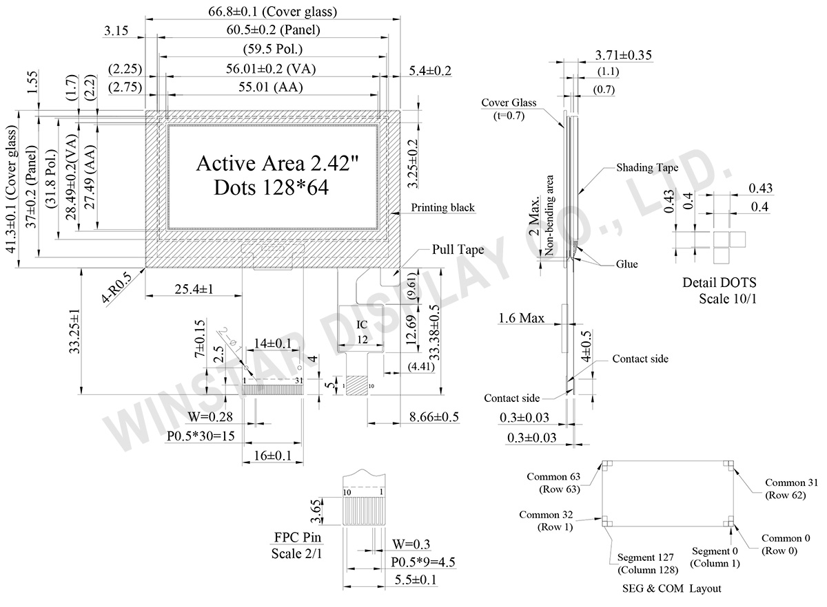
Dane mechaniczne
| Rzecz | Wymiar | Jednostka |
|---|---|---|
| Matryca punktowa | 128 x 64 | pikseli |
| Wymiary modułu | 66.8 × 41.3 × 3.71 | mm |
| Obszar aktywny | 55.01 × 27.49 | mm |
| Wielkość piksela | 0.40 × 0.40 | mm |
| Raster pomiędzy pikselami | 0.43 × 0.43 | mm |
| Tryb wyświetlania | matryca | |
| Kolor wyświetlacza | Monochromatyczny | |
| Interfejs | 8Bits 68xx 80xx / 4-Wire SPI / I2C | |
| Drive Duty | 1/64 Duty | |
| OLED IC | SSD1309 | |
| Rozmiar | 2.42 cale | |
| CTP IC | GT911 | |
| Detect Point | 1 | |
| CTP Interfejs | I2C | |
| Powierzchnia | Glare | |
Bezwzględne oceny maksymalne
| Parameter | Symbol | Minimalna wartość | Maksymalna wartość | Jednostka |
|---|---|---|---|---|
| Supply Voltage for Logic | VDD | -0.3 | 4 | V |
| Supply Voltage for Display | VCC | 0 | 15 | V |
| Temperatura pracy | TOP | -20 | +70 | °C |
| Temperatura przechowywania | TSTG | -30 | +80 | °C |
Parametry elektryczne
DC Parametry elektryczne
| Rzecz | Symbol | Stan | Minimalna wartość | Typowa wartość | Maksymalna wartość | Jednostka |
|---|---|---|---|---|---|---|
| Supply Voltage for Logic | VDD | - | 2.8 | 3.0 | 3.3 | V |
| Supply Voltage for Display | VCC | - | 12.5 | 13.0 | 13.5 | V |
| High Level Input | VIH | - | 0.8×VDD | - | - | V |
| Low Level Input | VIL | - | - | - | 0.2×VDD | V |
| High Level Output | VOH | - | 0.9×VDD | - | - | V |
| Low Level Output | VOL | - | - | - | 0.1×VDD | V |
| 50% Check Board operating Current | VCC =13.0V | - | 25 | 36 | mA | |
Touch Panel Controller GT911
| Rzecz | Symbol | Minimalna wartość | Typowa wartość | Maksymalna wartość | Jednostka |
|---|---|---|---|---|---|
| Supply Voltage | VDD | 2.8 | 3.0 | 3.3 | V |
| Input High Volt. | VIH | 0.75xVDD | VDD+0.3 | V | |
| Input Low Volt. | VIL | -0.3 | - | 0.25xVDD | V |
| Output High Volt. | VOH | 0.85xVDD | - | - | V |
| Output Low Volt. | VOL | - | - | 0.15xVDD | V |
")

