Funzione dei Pin di Interfaccia
Funkcja pinów interfejsu
| Pin No. |
Simbolo |
I/O |
Funzione |
| 1 |
VCOM |
P |
Common Voltage |
| 2~3 |
VDD |
P |
Power Supply |
| 4~6 |
NC |
- |
No connection |
| 7 |
GND |
P |
Ground |
| Pin No. |
Symbol |
I/O |
Funkcja |
| 1 |
VCOM |
P |
Common Voltage |
| 2~3 |
VDD |
P |
Power Supply |
| 4~6 |
NC |
- |
No connection |
| 7 |
GND |
P |
Ground |
| 8 |
Rxin0- |
I |
-LVDS Differential Data Input |
| 9 |
Rxin0+ |
I |
+LVDS Differential Data Input |
| 10 |
GND |
P |
Ground |
| 11 |
Rxin1- |
I |
-LVDS Differential Data Input |
| 12 |
Rxin1+ |
I |
+LVDS Differential Data Input |
| 13 |
GND |
P |
Ground |
| 14 |
Rxin2- |
I |
-LVDS Differential Data Input |
| 15 |
Rxin2+ |
I |
+LVDS Differential Data Input |
| 16 |
GND |
P |
Ground |
| 17 |
RxCLK- |
I |
-LVDS Differential Clock Input |
| 18 |
RxCLK+ |
I |
+LVDS Differential Clock Input |
| 19 |
GND |
P |
Ground |
| 20 |
Rxin3- |
I |
-LVDS Differential Data Input |
| 21 |
Rxin3+ |
I |
+LVDS Differential Data Input |
| 22 |
GND |
P |
Ground |
| 23~24 |
NC |
- |
No connection |
| 25 |
GND |
P |
Ground |
| 26~28 |
NC |
- |
No connection |
| 29 |
AVDD |
P |
Power for Analog Circuit |
| 30 |
GND |
P |
Ground |
| 31~34 |
NC |
- |
No connection |
| 35 |
VGL |
P |
Gate OFF Voltage |
| 36~37 |
NC |
- |
No connection |
| 38 |
VGH |
P |
Gate ON Voltage |
| 39~40 |
NC |
- |
No connection |
I: input, O: output, P: Power
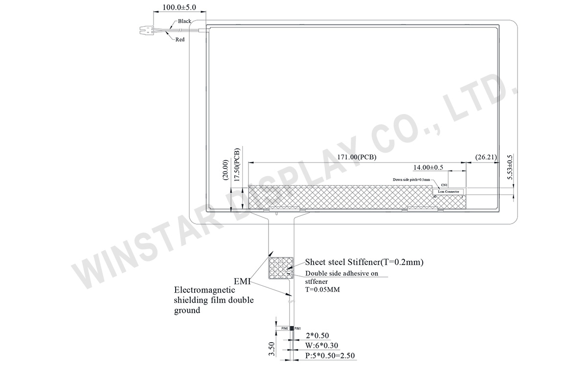
PCAP PIN Definition
| Pin |
Symbol |
Funkcja |
| 1 |
SDA |
I2C data input and output |
| 2 |
SCL |
I2C clock input |
| 3 |
RST |
External Reset, Low is active |
| 4 |
INT |
External interrupt to the host |
| 5 |
VDDT |
Power Supply : +3.3V |
| 6 |
GND |
Ground for analog circuit |
Ogólna specyfikacja
| Rzecz |
Wymiar |
Jednostka |
| Rozmiar |
10.1 |
calowy |
| Matryca punktowa |
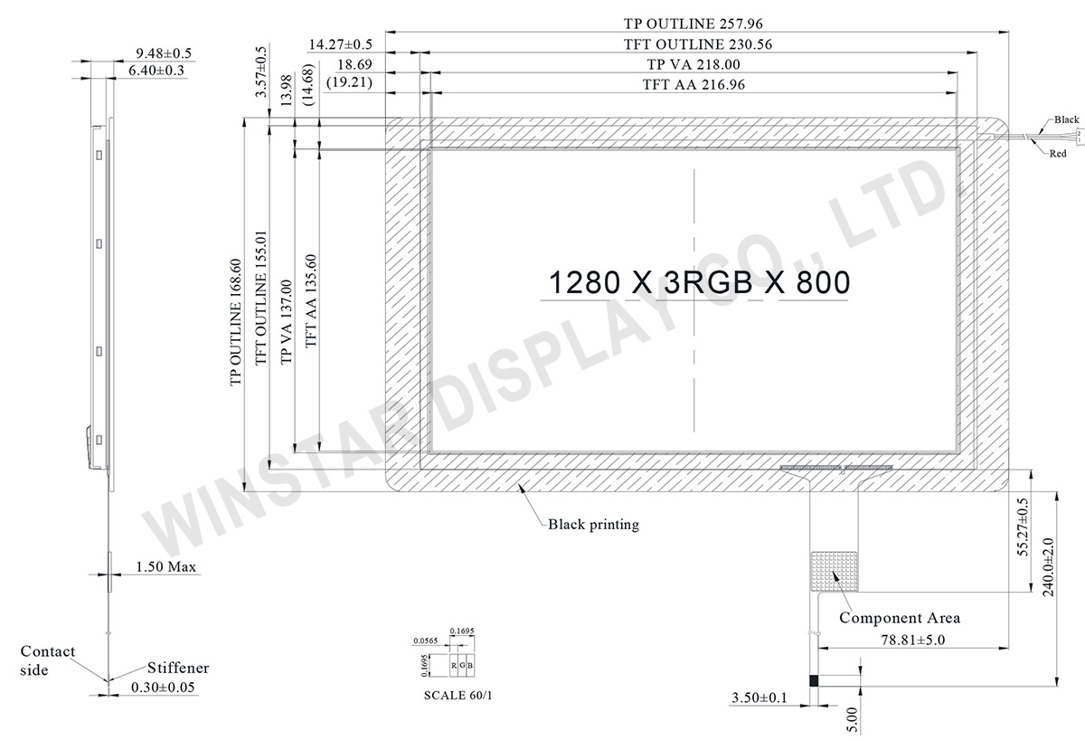
1280 × 3(RGB) × 800 |
dots |
| Wymiary modułu |
257.96 × 168.6 × 9.48 |
mm |
| Obszar aktywny |
216.96 (H) × 135.6(V) |
mm |
| Raster pomiędzy pikselami |
0.1695 × 0.1695 |
mm |
| Tryb wyświetlania |
czarny |
| Pixel Arrangement |
R.G.B. Vertical Stripe |
| Rodzaj podświetlenia |
LED, biały |
| Proporcje |
16:9 |
| Interfejs (Logic) |
LVDS |
| PCAP IC |
GT928 albo odpowiednik |
| PCAP Interfejs |
I2C |
| PCAP FW Version |
0X50 |
| Panel dotykowy |
Pojemnościowy panel dotykowy (PCAP) |
| Powierzchnia |
Glare |
Bezwzględne oceny maksymalne
| Rzecz |
Symbol |
Minimalna wartość |
Typowa wartość |
Maksymalna wartość |
Jednostka |
| Temperatura pracy |
TOP |
-20 |
- |
+70 |
℃ |
| Temperatura przechowywania |
TST |
-20 |
- |
+70 |
℃ |
Parametry elektryczne
| Rzecz |
Symbol |
Standardowa wartość |
Jednostk |
| Minimalna wartość |
Typowa |
Maksymalna wartość |
| Power voltage |
VDD |
2.3 |
2.5 |
2.7 |
V |
| AVDD |
8.0 |
8.2 |
8.4 |
V |
| VGH |
21.7 |
22 |
22.3 |
V |
| VGL |
-7.3 |
-7 |
-6.7 |
V |
| Input signal voltage |
VCOM |
2.7 |
3.0 |
3.3 |
V |
| Supply Voltage For Touch Logic |
VDDT |
2.8 |
- |
3.3 |
V |
8 Rxin0- I -LVDS Differential Data Input 9 Rxin0+ I +LVDS Differential Data Input 10 GND P Ground 11 Rxin1- I -LVDS Differential Data Input 12 Rxin1+ I +LVDS Differential Data Input 13 GND P Ground 14 Rxin2- I -LVDS Differential Data Input 15 Rxin2+ I +LVDS Differential Data Input 16 GND P Ground 17 RxCLK- I -LVDS Differential Clock Input 18 RxCLK+ I +LVDS Differential Clock Input 19 GND P Ground 20 Rxin3- I -LVDS Differential Data Input 21 Rxin3+ I +LVDS Differential Data Input 22 GND P Ground 23~24 NC - No connection 25 GND P Ground 26~28 NC - No connection 29 AVDD P Power for Analog Circuit 30 GND P Ground 31~34 NC - No connection 35 VGL P Gate OFF Voltage 36~37 NC - No connection 38 VGH P Gate ON Voltage 39~40 NC - No connection
I: input, O: output, P: Power
PCAP PIN Definition
| Pin |
Symbol |
Function |
| 1 |
SDA |
I2C data input and output |
| 2 |
SCL |
I2C clock input |
| 3 |
RST |
External Reset, Low is active |
| 4 |
INT |
External interrupt to the host |
| 5 |
VDDT |
Power Supply : +3.3V |
| 6 |
GND |
Ground for analog circuit |
Specifiche generali
| Articolo |
Dimensioni |
Unità |
| Dimensione |
10.1 |
pollici |
| A matrice di punti |
1280 × 3(RGB) × 800 |
dots |
| Dimensione del modulo |
257.96 × 168.6 × 9.48 |
mm |
| Area attiva |
216.96 (H) × 135.6(V) |
mm |
| Passo del Dot |
0.1695 × 0.1695 |
mm |
| Modalità display |
Nero |
| Pixel Arrangement |
R.G.B. Vertical Stripe |
| Tipo di backlight |
LED, Bianco |
| Proporzioni dell’area visiva (ratio) |
16:9 |
| Interfaccia (Logic) |
LVDS |
| PCAP IC |
GT928 или эквивалентный |
| PCAP Interfaccia |
I2C |
| PCAP FW versione |
0X50 |
| Con / senza Touch Panel |
con pannello touch capacitivo (PCAP) |
| Superficie |
Bagliore (Glare) |
Valori massimi assoluti
| Articolo |
Simbolo |
Valore Min |
Valore tipico |
Valore massimo |
Unità |
| Temperatura di lavoro |
TOP |
-20 |
- |
+70 |
℃ |
| Temperatura di stock |
TST |
-20 |
- |
+70 |
℃ |
Caratteristiche elettriche
| Articolo |
Simbolo |
Valore standard |
Unità |
| Valore Min |
Valore tipico |
Valore massimo |
| Power voltage |
VDD |
2.3 |
2.5 |
2.7 |
V |
| AVDD |
8.0 |
8.2 |
8.4 |
V |
| VGH |
21.7 |
22 |
22.3 |
V |
| VGL |
-7.3 |
-7 |
-6.7 |
V |
| Input signal voltage |
VCOM |
2.7 |
3.0 |
3.3 |
V |
| Supply Voltage For Touch Logic |
VDDT |
2.8 |
- |
3.3 |
V |