


Wyświetlacz LVDS IPS PCAP TFT 10.1" 1024x600
Numer modelu WF101JSYAHLNB0
►Rozmiar : 10.1”
►Rozdzielczość : 1024×600 punktów
►Godzina obserwacji: IPS
►Interfejs : LVDS
►Kontroler : EK79001HN + EK73215BCGA
►Płyta kontrolera : brake
►Brightness(cd/m2) : 900
►Otwory w ramie : brak
►Panel dotykowy : Pojemnościowy panel dotykowy (PCAP)
►Detect Point : 5 Fingers
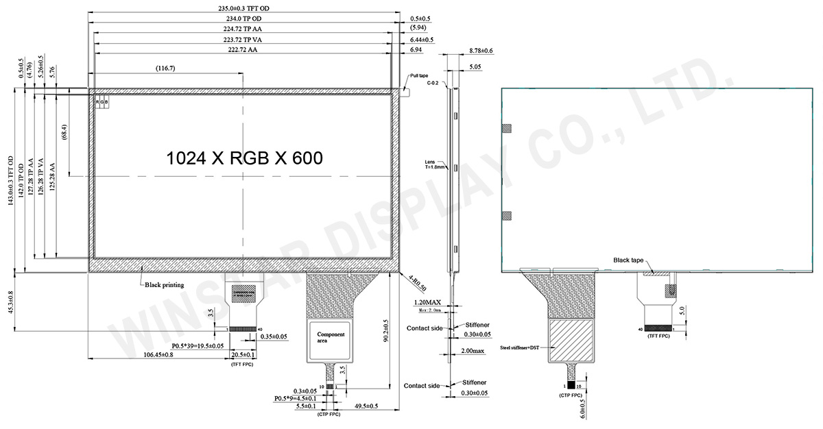
Rysunek
Specyfikacja
Funkcja pinów interfejsu
| Pin No. | Symbol | Funkcja |
|---|---|---|
| 1 | VCOM | Common voltage |
| 2 | VDD | Digital power |
| 3 | VDD | Digital power |
| 4 | NC | Not connect |
| 5 | Reset | Global reset pin. Active low to enter reset state. Suggest to connecting with an RC reset circuit for stability. Normally pull high. (R=10KΩ,C=1μF) |
| 6 | STBYB | Standby mode, normally pull high STBYB=”1”, normal operation STBYB=”0”,timing control, source driver will turn off, all output are high-Z |
| 7 | GND | Digital ground |
| 8 | RXIN0- | Negative LVDS differential data inputs |
| 9 | RXIN0+ | Positive LVDS differential data inputs |
| 10 | GND | Digital ground |
| 11 | RXIN1- | Negative LVDS differential data inputs |
| 12 | RXIN1+ | Positive LVDS differential data inputs |
| 13 | GND | Digital ground |
| 14 | RXIN2- | Negative LVDS differential data inputs |
| 15 | RXIN2+ | Positive LVDS differential data inputs |
| 16 | GND | Digital ground |
| 17 | RXCLKN- | Negative LVDS differential clock inputs |
| 18 | RXCLKN+ | Positive LVDS differential clock inputs |
| 19 | GND | Digital ground |
| 20 | RXIN3- | Negative LVDS differential data inputs |
| 21 | RXIN3+ | Positive LVDS differential data inputs |
| 22 | GND | Digital ground |
| 23 | NC | Not connect |
| 24 | NC | Not connect |
| 25 | GND | Digital ground |
| 26 | NC | Not connect |
| 27 | NC | Not connect |
| 28 | SELB | 6-bit/8-bit input select SELB = L , 8-bit ; SELB = H , 6-bit |
| 29 | AVDD | Analog power |
| 30 | GND | Digital ground |
| 31 | LED- | LED Cathode |
| 32 | LED- | LED Cathode |
| 33 | L/R | Left or right display control |
| 34 | U/D | Up / down display control |
| 35 | VGL | Negative power for TFT |
| 36 | NC | Not connect |
| 37 | NC | Not connect |
| 38 | VGH | Positive power for TFT |
| 39 | LED+ | LED Anode |
| 40 | LED+ | LED Anode |
When L/R=”1”,set left to right scan direction.
When U/D=”0”,set top to bottom scan direction.
When U/D=”1”,set bottom to top scan direction.
PCAP PIN Definition
| Pin | Symbol | Funkcja |
|---|---|---|
| 1 | USB_VSS | System ground |
| 2 | USB_VDD 5V | Power supply |
| 3 | USB_D+ | Data + |
| 4 | USB_D- | Data - |
| 5 | VSS | System ground |
| 6 | SDA | I2C data input and output |
| 7 | SCL | I2C clock input |
| 8 | RST | External Reset, Low is active |
| 9 | INT | External interrupt to the host |
| 10 | VDDT 3.3 | Power supply |
Ogólna specyfikacja
| Rzecz | Wymiar | Jednostka |
|---|---|---|
| Rozmiar | 10.1 | cale |
| Matryca punktowa | 1024 RGB x 600 | dots |
| Wymiary modułu | 235(W) x 143(H) x 8.78(D) | mm |
| Obszar aktywny | 222.72 (H) x 125.28(V) | mm |
| Raster pomiędzy pikselami | 0.2175(W) x 0.2088(H) | mm |
| Rodzaj LCD | TFT, czarny, Transmisyjny | |
| Interfejs | LVDS | |
| Kontroler | EK79001HN + EK73215BCGA albo odpowiednik | |
| godzina obserwacji | 85/85/85/85 | |
| Proporcje | 16:9 | |
| Rodzaj podświetlenia | LED, biały | |
| PCAP IC | ILI2511 albo odpowiednik | |
| PCAP Interfejs | USB (I2C available) | |
| PCAP FW Version | V6.0.0.0.62.90.1.2 | |
| Panel dotykowy | PCAP | |
| Powierzchnia | Glare | |
Bezwzględne oce
| Rzecz | Symbol | Minimalna wartość | Typowa wartość | Maksymalna wartość | Jednostka |
|---|---|---|---|---|---|
| Temperatura pracy | TOP | -20 | - | +70 | ℃ |
| Temperatura przechowywania | TST | -30 | - | +80 | ℃ |
Parametry elektryczne
Typical Operation Conditions (At Ta = 25 °C,)
| Rzecz | Symbol | Minimalna wartość | Typowa wartość | Maksymalna wartość | Jednostka |
|---|---|---|---|---|---|
| Digital Power Supply Voltage For LCD | VDD | 3 | 3.3 | 3.6 | V |
| Analog Power Supply Voltage | AVDD | 9.89 | 10.2 | 10.5 | V |
| Gate On Power Supply Voltage | VGH | 19.4 | 20.0 | 20.6 | V |
| Gate Off Power Supply Voltage | VGL | -10.3 | -10.0 | -9.7 | V |
| Common Power Supply Voltage | VCOM | 4.0 | 4.3 | 4.6 | V |
| Input logic high voltage | VIH | 0.7 VDD | - | VDD | V |
| Input logic low voltage | VIL | 0 | - | 0.3 VDD | V |
| Supply PCAP | USB_VDD 5V | 4.4 | 5.0 | 5.5 | V |
| I VDD 5V | — | 97.8 | 120 | mA |

")


