


2.8 inch 240x320 TFT IPS LCD Display
Model No. WF28JTYAJDNN0
►Size: 2.8"
►Resolution: 240×320 dots
►View Direction: IPS
►Interface: MCU, SPI
►TFT Driver IC: ILI9341
►Control-Board: No
►Brightness(cd/m²): 500
►Frame Through Hole: No
►Touch Screen: Without Touch Screen
DESCRIPTION
WF28J is a 2.8 inch wider view angle IPS TFT LCD module, with resolution 240x320 pixels. WF28J module is a portrait mode IPS TFT-LCD; this module is built in with ILI9341 controller IC; it supports MCU 8-bit/16-bit or SPI interface, contrast ratio 800 (typical value). The brightness of WF28JTYAJDNN0 is 500 nits (typical value). This 2.8” IPS TFT has a wider viewing angle than TN TFT, the view angle is Left:80 / Right:80 / Up:80 / Down:80 degree (typical value). The supply voltage for interface logic (IOVCC) of WF28J model is from 1.65V to 3.3V, supply for analog circuit is from 2.5V ~3.3V, normally black, transmissive LCD type, aspect ratio 3:4, glare surface glass. It can be operating at temperatures from -20℃ to +70℃ and storage temperatures from -30℃ to +80℃.
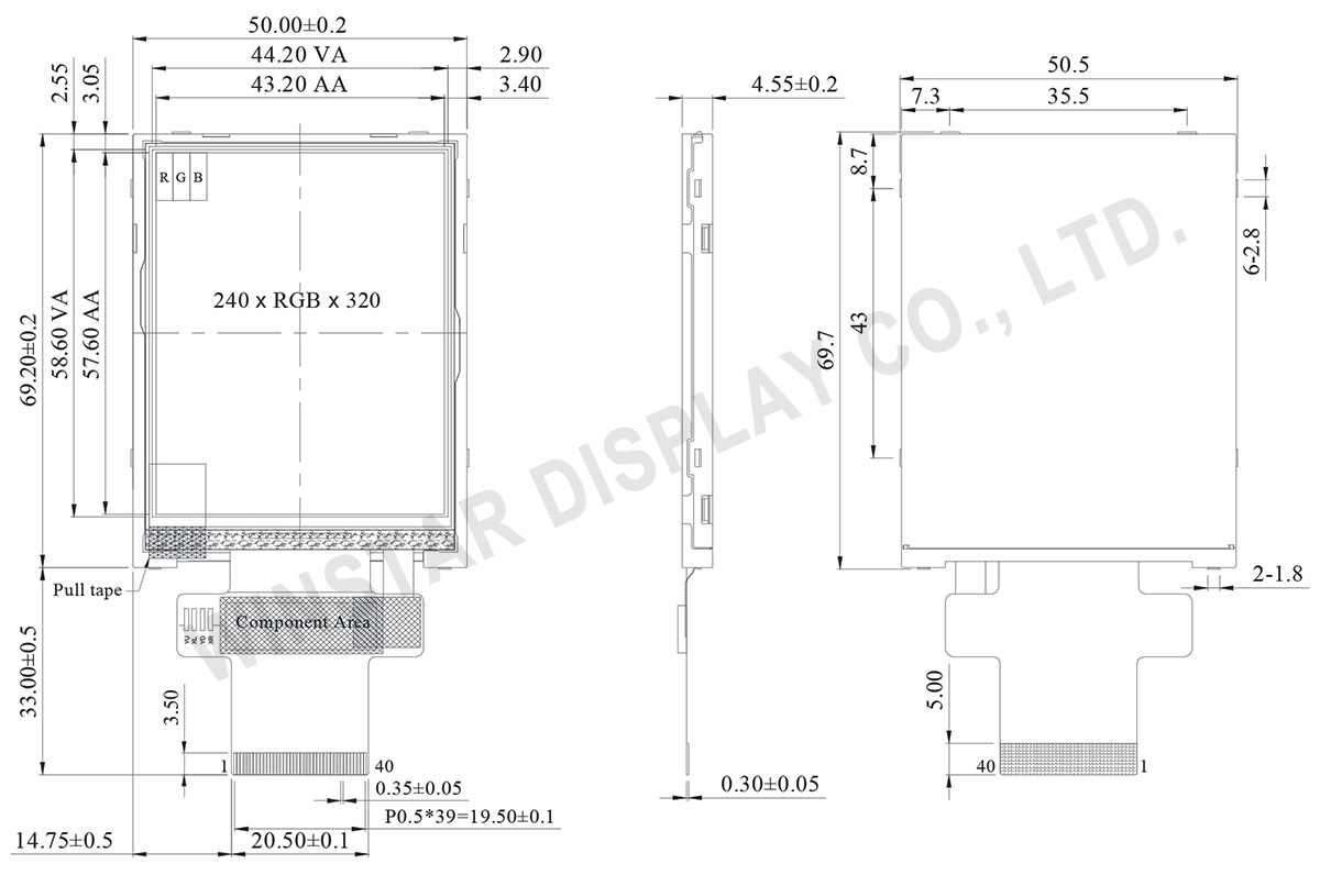
DRAWING
SPECIFICATIONS
Interface Pin Function
LCM PIN Definition
| NO | Symbol | Function | I/O | ||||||||||||||||||||||||||||||||||||||||||||
|---|---|---|---|---|---|---|---|---|---|---|---|---|---|---|---|---|---|---|---|---|---|---|---|---|---|---|---|---|---|---|---|---|---|---|---|---|---|---|---|---|---|---|---|---|---|---|---|
| 1 | GND | Ground | P | ||||||||||||||||||||||||||||||||||||||||||||
| 2-6 | NC | No connection | - | ||||||||||||||||||||||||||||||||||||||||||||
| 7 | VCI | High voltage power supply for analog circuit blocks (2.5 ~ 3.3 V) |
P | ||||||||||||||||||||||||||||||||||||||||||||
| 8 | IOVCC | Low voltage power supply for interface logic circuits (1.65 ~ 3.3 V) |
P | ||||||||||||||||||||||||||||||||||||||||||||
| 9 | TE | Tearing effect output pin to synchronize MPU to frame writing, activated by S/W command. When this pin is not activated, this pin is low. If not used, open this pin. |
O | ||||||||||||||||||||||||||||||||||||||||||||
| 10 | CS | Chip select signal. | I | ||||||||||||||||||||||||||||||||||||||||||||
| 11 | D/CX(SCL) | (D/CX): This pin is used to select “Data or Command” in the parallel interface. When DCX = 1, data is selected. When DCX = 0, command is selected. (SCL): This pin is used as the serial interface clock in 3-wire 9-bit/4-wire 8-bit serial data interface. If not used, this pin should be connected to VDDI or VSS. |
I | ||||||||||||||||||||||||||||||||||||||||||||
| 12 | WR(SPI_D/C) | (WRX) - 8080-Ⅰ/8080-Ⅱ system: Serves as a write signal and writes data at the rising edge. (D/CX) - 4-line system: Serves as the selector of command or parameter. Fix to VDDI level when not in use. |
I | ||||||||||||||||||||||||||||||||||||||||||||
| 13 | RD | 8080-Ⅰ/8080-Ⅱ system (RDX): Serves as a read signal and MCU read data at the rising edge. Fix to VDDI level when not in use. |
I | ||||||||||||||||||||||||||||||||||||||||||||
| 14-29 | DB0~DB15 | 18-bit parallel bi-directional data bus for MCU system and RGB interface mode Fix to VSS level when not in use. |
I/O | ||||||||||||||||||||||||||||||||||||||||||||
| 30 | RESET | This signal will reset the device and must be applied to properly initialize the chip. Signal is active low. |
I | ||||||||||||||||||||||||||||||||||||||||||||
| 31 | IM0 | Select the MCU interface mode
If use RGB Interface must select serial interface. * : Fix this pin at VDDI or VSS. |
I | ||||||||||||||||||||||||||||||||||||||||||||
| 32 | IM1 | ||||||||||||||||||||||||||||||||||||||||||||||
| 33 | IM2 | ||||||||||||||||||||||||||||||||||||||||||||||
| 34 | DB16 | 18-bit parallel bi-directional data bus for MCU system and RGB interface mode Fix to VSS level when not in use. |
I/O | ||||||||||||||||||||||||||||||||||||||||||||
| 35 | DB17 | ||||||||||||||||||||||||||||||||||||||||||||||
| 36 | LEDK | Cathode of LED backlight. | P | ||||||||||||||||||||||||||||||||||||||||||||
| 37 | LEDK | Cathode of LED backlight. | P | ||||||||||||||||||||||||||||||||||||||||||||
| 38 | LEDA | Anode of LED backlight. | P | ||||||||||||||||||||||||||||||||||||||||||||
| 39 | SDI(SDA) | When IM[3] : Low, Serial in/out signal. When IM[3] : High, Serial input signal. The data is applied on the rising edge of the SCL signal. If not used, fix this pin at VDDI or VSS. |
I/O | ||||||||||||||||||||||||||||||||||||||||||||
| 40 | SDO | Serial output signal. The data is outputted on the falling edge of the SCL signal. If not used, open this pin |
O | ||||||||||||||||||||||||||||||||||||||||||||
General Specifications
| Item | Dimension | Unit |
|---|---|---|
| Size | 2.8 | inch |
| Dot Matrix | 240 x RGB x 320(TFT) | dots |
| Module dimension | 50.5(W) x 69.7(H) x 4.55(D) | mm |
| Active area | 43.2 x 57.6 | mm |
| Dot pitch | 0.18 x 0.18 | mm |
| LCD type | TFT, Normally Black, Transmissive | |
| TFT Driver IC | ILI9341V or equivalent | |
| TFT Interface | MCU/SPI | |
| Viewing angle | 80/80/80/80 | |
| Aspect Ratio | 3:4 | |
| Backlight Type | LED,Normally White | |
| Touch Panel | Without Touch Panel | |
| Surface | Glare | |
Absolute Maximum Ratings
| Item | Symbol | Min | Typ | Max | Unit |
|---|---|---|---|---|---|
| Operating Temperature | TOP | -20 | - | +70 | ℃ |
| Storage Temperature | TST | -30 | - | +80 | ℃ |
Electrical Characteristics
| Item | Symbol | Condition | Min | Typ | Max | Unit |
|---|---|---|---|---|---|---|
| Supply Voltage for digital | IOVCC | - | 1.65 | - | 3.3 | V |
| Supply Voltage for analog | VCI | - | 2.5 | - | 3.3 | V |
| Power Supply for Current | ICC | IOVCC=VCI =VCC=3.28V |
- | 12 | 18 | mA |
Search keyword: tft 2.8, tft 2.8", 2.8 tft lcd, 2.8" tft lcd, 2.8 inch tft lcd, tft lcd 2.8, 2.8 tft display, 2.8" tft display, 2.8 inch tft display, tft display 2.8, tft display 2.8"


