WF50FTWAGLNN0 is a 5 inch IPS landscape mode TFT LCD module, with resolution 800x480 pixels. WF50FTWAGLNN0 module is built in with ST7262 driver IC; this module supports LVDS interface (Default VESA), contrast ratio 1,000:1 (typical value), brightness 500 nits (typical value). If customers require RGB interface, please choose WF50FTWAGDNN0.
This 5" IPS TFT has a wider viewing angle than TN TFT, the view angle is Left:80 / Right:80 / Up:80 / Down:80 degree (typical value). The power voltage of WF50F model is from 3.1 to 3.6V, typical value 3.3V, aspect ratio 16:9, normally black, transmissive LCD type, anti-glare surface glass. It can be operating at temperatures from -30℃ to +80℃ and storage temperatures from -30℃ to +80℃. WF50F have Resistive Touch Panel and Projected Capacitive Touch Panel for optional.
SPECIFICATIONS
Interface
| Pin |
Symbol |
Function |
| 1 |
NC |
No connection |
| 2 |
VCC |
Power voltage |
| 3 |
VCCI |
Power supply for digital I/O pins. |
| 4 |
NC |
No connection |
| 5 |
GRB |
Global reset pin. When GRB is “L”, internal initialization procedure is executed |
| 6 |
DISP |
Display on/off |
| 7 |
GND |
Power Ground |
| 8 |
RXIN0- |
LVDS input lane: RX0-/ RX0+ |
| 9 |
RXIN0+ |
| 10 |
GND |
Power Ground |
| 11 |
RXIN1- |
LVDS input lane: RX1-/ RX1+ |
| 12 |
RXIN1+ |
| 13 |
GND |
Power Ground |
| 14 |
RXIN2- |
LVDS input lane: RX2-/ RX2+ |
| 15 |
RXIN2+ |
| 16 |
GND |
Power Ground |
| 17 |
RXCLKIN- |
LVDS input lane, detail pin define please refer to LVDS
Input Pin Mapping Table. |
| 18 |
RXCLKIN+ |
| 19 |
GND |
Power Ground |
| 20 |
RXIN3- |
LVDS input lane: RX3-/ RX3+ |
| 21 |
RXIN3+ |
| 22 |
GND |
Power Ground |
| 23-24 |
NC |
No connection |
| 25 |
FMT |
LVDS_FMT sets LVDS data format.
| LVDS_FMT |
Function Description |
| L |
VESA Mode (Default) |
| H |
JEIDA Mode |
LVDS_FMT is not used in RGB interface and should be connected to “L”. |
| 26-27 |
NC |
No connection |
| 28 |
SELB |
SELB sets VSYNC polarity in RGB interface and sets LVDS 3- / 4- lane in LVDS interface.
| MCU Type |
VDPOL |
Function Description |
| RGB interface |
L |
VSYNC polarity: positive |
| H |
VSYNC polarity: positive: negative (Default) |
| LVDS inteface |
L |
LVD 3 lane |
| H |
LVD 4 lane (Default) |
|
| 29 |
NC |
No connection |
| 30 |
GND |
Power Ground |
| 31-32 |
VLED- |
Power for LED backlight (Cathode) |
| 33 |
L/R |
Horizontal scan direction control pin. This pin must be connected to “H” or “L” according to system application
| HDIR |
Function Description |
| L |
From right to left |
| H |
From left to right (Default) |
|
| 34 |
U/D |
Vertical scan direction control pin. This pin must be connected to “H” or “L” according to system application.
| VDIR |
Function Description |
| L |
From down to up. |
| H |
From up to down.(Default) |
|
| 35 |
NC |
No connection |
| 36-37 |
GND |
Power Ground |
| 38 |
NC |
No connection |
| 39-40 |
VLED+ |
Power for LED backlight (Anode) |
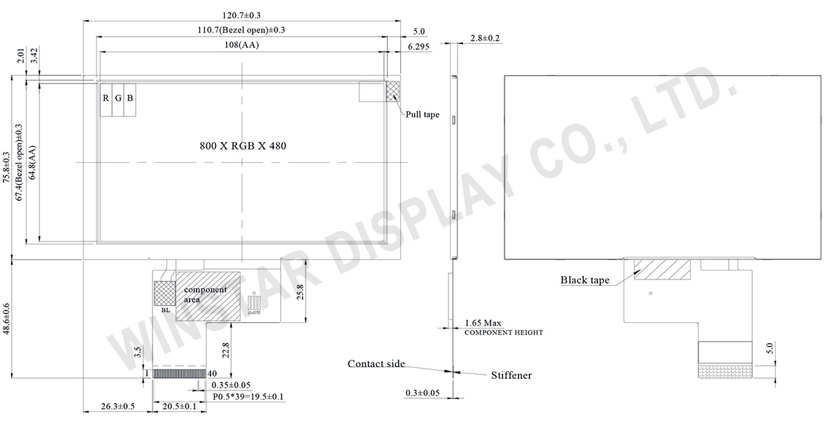
General Specifications
| Item |
Dimension |
Unit |
| Size |
5.0 |
inch |
| Dot Matrix |
800× 3(RGB) × 480 |
dots |
| Module dimension |
120.7(W) ×75.8(H) ×2.8mm |
mm |
| Active area |
108(W) ×64.8 (H) mm |
mm |
| Dot pitch |
0.135(W) ×0.135(H) mm |
mm |
| LCD type |
TFT, Normally Black, Transmissive |
| View Direction |
80/80/80/80 |
| Aspect Ratio |
16:9 |
| Driver IC |
ST7262 or equivalent |
| Interface |
LVDS |
| Backlight Type |
LED ,Normally White |
| Touch Panel |
Without Touch Panel |
| Surface |
Anti-Glare |
Absolute Maximum Ratings
| Item |
Symbol |
Min |
Typ |
Max |
Unit |
| Operating Temperature |
TOP |
-30 |
- |
+80 |
℃ |
| Storage Temperature |
TST |
-30 |
- |
+80 |
℃ |
Electrical Characteristics
Typical Operation Conditions
| Item |
Symbol |
Values |
Unit |
| Min. |
Typ. |
Max. |
| Power voltage |
VCC |
3.1 |
3.3 |
3.6 |
V |
| Power voltage |
VCCI |
3.1 |
3.3 |
3.6 |
V |
| Current for Driver(Black) |
ICC |
- |
67.6 |
102 |
mA |
Search keyword: tft 5", 5 tft lcd, 5" tft lcd, 5 inch tft lcd, tft lcd 5, 5 tft display, 5" tft display, 5 inch tft display, tft display 5, tft display 5"