Interface
LCM PIN Definition
| Pin No. |
Symbol |
I/O |
Description |
| 1 |
IF1 |
I |
Input data format control (Note1) |
| 2 |
IF2 |
I |
Input data format control (Note1) |
| 3 |
POL |
O |
Polarity Signal connect to VCOM driving circuit. |
| 4 |
RESET |
I |
Hardware reset. |
| 5 |
SPENA |
I |
Chip select |
| 6 |
SPCL |
I |
Serial Clock |
| 7 |
SPDA |
I/O |
Serial Data |
| 8 |
B0 |
I |
Blue Data bit (LSB) |
| 9 |
B1 |
I |
Blue Data bit |
| 10 |
B2 |
I |
Blue Data bit |
| 11 |
B3 |
I |
Blue Data bit |
| 12 |
B4 |
I |
Blue Data bit |
| 13 |
B5 |
I |
Blue Data bit |
| 14 |
B6 |
I |
Blue Data bit |
| 15 |
B7 |
I |
Blue Data bit(MSB) |
| 16 |
G0 |
I |
Green Data bit(LSB) |
| 17 |
G1 |
I |
Green Data bit |
| 18 |
G2 |
I |
Green Data bit |
| 19 |
G3 |
I |
Green Data bit |
| 20 |
G4 |
I |
Green Data bit |
| 21 |
G5 |
I |
Green Data bit |
| 22 |
G6 |
I |
Green Data bit |
| 23 |
G7 |
I |
Green Data bit(MSB) |
| 24 |
R0 |
I |
Red Data bit(LSB) |
| 25 |
R1 |
I |
Red Data bit |
| 26 |
R2 |
I |
Red Data bit |
| 27 |
R3 |
I |
Red Data bit |
| 28 |
R4 |
I |
Red Data bit |
| 29 |
R5 |
I |
Red Data bit |
| 30 |
R6 |
I |
Red Data bit |
| 31 |
R7 |
I |
Red Data bit(MSB) |
| 32 |
Hsync |
I |
Horizontal synchronous signal |
| 33 |
Vsync |
I |
Vertical synchronous signal |
| 34 |
Data CLK |
I |
Dot data clock |
| 35 |
AVDD |
I |
4.5V~5.5V |
| 36 |
AVDD |
I |
4.5V~5.5V |
| 37 |
Vcc |
I |
3V~3.6V |
| 38 |
Vcc |
I |
3V~3.6V |
| 39 |
NPC |
O |
NTSC/PAL mode Auto detection result H:NTSC/L:PAL |
| 40 |
VGL |
I |
Gate off power |
| 41 |
VGL |
I |
Gate off power |
| 42 |
UD |
I |
Up/Down scan setting. H: Reverse scan / L: Normal scan |
| 43 |
VGH |
I |
Gate on power |
| 44 |
LRC |
I |
Shift direction of device internal shift register control. |
| 45 |
GND |
I |
GROUND |
| 46 |
VCOM |
I |
VCOM driving input |
| 47 |
VCOM |
I |
VCOM driving input |
| 48 |
ENB |
I |
Data enable input. Normally pull low. |
| 49 |
GND |
I |
GROUND |
| 50 |
GND |
I |
GROUND |
Note:
| IF2,IF1 |
Input data format |
| L,L(default) |
Serial RGB |
| L,H |
Parallel RGB |
| H,L |
CCIR601 |
| H,H |
CCIR656 |
Backlight PIN Definition
| Pin No. |
Symbol |
I/O |
Description |
| 1 |
VLED+ |
I |
Red, LED_ Anode |
| 2 |
VLED- |
I |
Black, LED_ Cathode |
PCAP PIN Definition
| Pin |
Symbol |
Function |
| 1 |
VSS |
Ground for analog circuit |
| 2 |
VDDT |
Power Supply : +3.3V |
| 3 |
SCL |
I2C clock input |
| 4 |
NC |
No connect |
| 5 |
SDA |
I2C data input and output |
| 6 |
NC |
No connect |
| 7 |
/RST |
External Reset, Low is active |
| 8 |
NC |
No connect |
| 9 |
/INT |
External interrupt to the host |
| 10 |
VSS |
Ground for analog circuit |
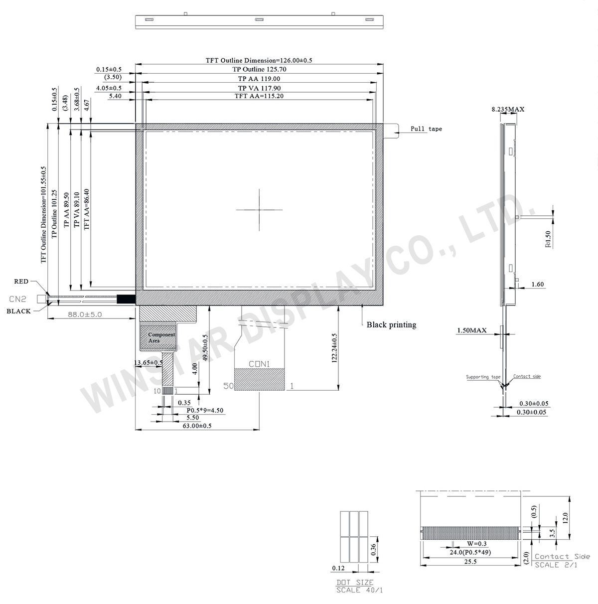
General Specifications
| Item |
Dimension |
Unit |
| Size |
5.7 |
inch |
| Dot Matrix |
320 × RGB × 240 (TFT) |
dots |
| Module dimension |
126.00(W) × 101.55(H) × 8.235(D) (MAX) |
mm |
| Active area |
115.2 × 86.40 |
mm |
| Dot pitch |
0.12 × 0.36 |
mm |
| LCD type |
TFT, Normally White, Transmissive |
| View Direction |
12 o'clock |
| Gray Scale Inversion Direction |
6 o'clock |
| Interface |
24-bit RGB |
| Aspect Ratio |
4:3 |
| Backlight Type |
LED, Normally White |
| PCAP FW Version |
FT5426 or Equivalent |
| PCAP Interface |
I2C |
| PCAP IC |
FN058A001_FT5426__V03_20180910_all.bin |
| Touch Panel |
Projected Capacitive Touch Panel (PCAP) |
| Surface |
Glare |
Absolute Maximum Ratings
| Item |
Symbol |
Min |
Typ |
Max |
Unit |
| Operating Temperature |
TOP |
-20 |
- |
+70 |
℃ |
| Storage Temperature |
TST |
-30 |
- |
+80 |
℃ |
Electrical Characteristics
| Item |
Symbol |
Condition |
Min |
Typ |
Max |
Unit |
| Supply Voltage For LCM |
VCC |
- |
3.0 |
3.3 |
3.6 |
V |
| Supply Voltage For CTP |
VDDT |
- |
2.8 |
- |
3.3 |
V |
| Input High Volt. |
VIH |
- |
0.7 VCC |
- |
VCC |
V |
| Input Low Volt. |
VIL |
- |
0 |
- |
0.3 VCC |
V |
| LCD Driving Supply Voltage |
VGH x 1 |
Ta=25℃ |
- |
15 |
- |
V x 3 |
| VGL x 2 |
- |
-10 |
- |
| VcomH |
2.5 |
- |
5.5 |
| VcomL |
-2.0 |
- |
0 |
| Supply Current For LCM |
IVCC |
VCC=3.3V |
- |
5 |
8 |
mA |
Search keyword: tft 5.7, tft 5.7", 5.7 tft lcd, 5.7" tft lcd, 5.7 inch tft lcd, tft lcd 5.7, 5.7 tft display, 5.7" tft display, 5.7 inch tft display, tft display 5.7, tft display 5.7"