


5.7" TFT con Schermoo Touch Capacitivo
Modello numero WF57DTIACDNGD
►Dimensione: 5.7 pollici
►Risoluzione : 320 x 240 punti
►Direzione di visione : 12H
►Interfaccia : RGB
►A bordo Controllore : --
►Scheda di controllo : Opzione
Luminosità (cd/m²) : 700
►Cornice di fissaggio: No
►Touch Screen : con schermoo touch capacitivo (PCAP)
►Detect Point : 5 Fingers
►O-Film : Opzione
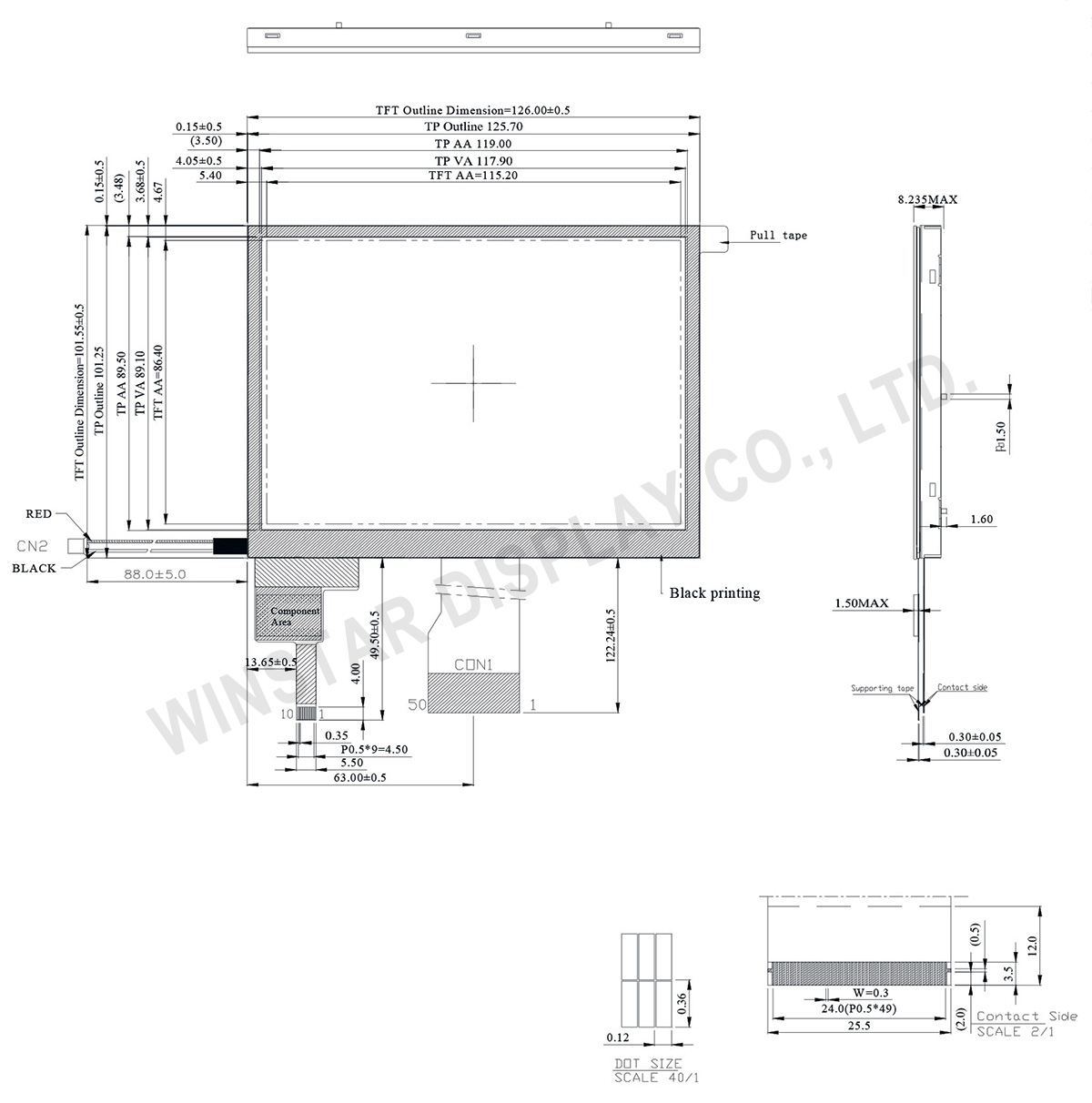
DISEGNO
SPECIFICHE TECNICHE
Funzione dei Pin di Interfaccia
LCM PIN Definition
| Pin No. | Simbolo | I/O | Funzione |
|---|---|---|---|
| 1 | IF1 | I | Input data format control (Note1) |
| 2 | IF2 | I | Input data format control (Note1) |
| 3 | POL | O | Polarity Signal connect to VCOM driving circuit. |
| 4 | RESET | I | Hardware reset. |
| 5 | SPENA | I | Chip select |
| 6 | SPCL | I | Serial Clock |
| 7 | SPDA | I/O | Serial Data |
| 8 | B0 | I | Blue Data bit (LSB) |
| 9 | B1 | I | Blue Data bit |
| 10 | B2 | I | Blue Data bit |
| 11 | B3 | I | Blue Data bit |
| 12 | B4 | I | Blue Data bit |
| 13 | B5 | I | Blue Data bit |
| 14 | B6 | I | Blue Data bit |
| 15 | B7 | I | Blue Data bit(MSB) |
| 16 | G0 | I | Green Data bit(LSB) |
| 17 | G1 | I | Green Data bit |
| 18 | G2 | I | Green Data bit |
| 19 | G3 | I | Green Data bit |
| 20 | G4 | I | Green Data bit |
| 21 | G5 | I | Green Data bit |
| 22 | G6 | I | Green Data bit |
| 23 | G7 | I | Green Data bit(MSB) |
| 24 | R0 | I | Red Data bit(LSB) |
| 25 | R1 | I | Red Data bit |
| 26 | R2 | I | Red Data bit |
| 27 | R3 | I | Red Data bit |
| 28 | R4 | I | Red Data bit |
| 29 | R5 | I | Red Data bit |
| 30 | R6 | I | Red Data bit |
| 31 | R7 | I | Red Data bit(MSB) |
| 32 | Hsync | I | Horizontal synchronous signal |
| 33 | Vsync | I | Vertical synchronous signal |
| 34 | Data CLK | I | Dot data clock |
| 35 | AVDD | I | 4.5V~5.5V |
| 36 | AVDD | I | 4.5V~5.5V |
| 37 | Vcc | I | 3V~3.6V |
| 38 | Vcc | I | 3V~3.6V |
| 39 | NPC | O | NTSC/PAL mode Auto detection result H:NTSC/L:PAL |
| 40 | VGL | I | Gate off power |
| 41 | VGL | I | Gate off power |
| 42 | UD | I | Up/Down scan setting. H: Reverse scan / L: Normal scan |
| 43 | VGH | I | Gate on power |
| 44 | LRC | I | Shift direction of device internal shift register control. |
| 45 | GND | I | GROUND |
| 46 | VCOM | I | VCOM driving input |
| 47 | VCOM | I | VCOM driving input |
| 48 | ENB | I | Data enable input. Normally pull low. |
| 49 | GND | I | GROUND |
| 50 | GND | I | GROUND |
| IF2,IF1 | Input data format |
|---|---|
| L,L(default) | Serial RGB |
| L,H | Parallel RGB |
| H,L | CCIR601 |
| H,H | CCIR656 |
Backlight PIN Definition
| Pin No. | Simbolo | I/O | Funzione |
|---|---|---|---|
| 1 | VLED+ | I | Red, LED_ Anode |
| 2 | VLED- | I | Black, LED_ Cathode |
PCAP PIN Definition
| Pin | Simbolo | Funzione |
|---|---|---|
| 1 | VSS | Ground for analog circuit |
| 2 | VDDT | Power Supply : +3.3V |
| 3 | SCL | I2C clock input |
| 4 | NC | No connect |
| 5 | SDA | I2C data input and output |
| 6 | NC | No connect |
| 7 | /RST | External Reset, Low is active |
| 8 | NC | No connect |
| 9 | /INT | External interrupt to the host |
| 10 | VSS | Ground for analog circuit |
Specifiche generali
| Articolo | Dimensioni | Unità |
|---|---|---|
| Dimensione | 5.7 | pollici |
| A matrice di punti | 320 × RGB × 240 (TFT) | dots |
| Dimensione del modulo | 126.00(W) × 101.55(H) × 8.235(D) (MAX) | mm |
| Area attiva | 115.2 × 86.40 | mm |
| Passo del Dot | 0.12 × 0.36 | mm |
| Tipo LCD | TFT, Bianco, Trasmissivo | |
| Direzione di visione | 12 o'clock | |
| Direzione di inversione della scala dei grigi | 6 o'clock | |
| Interfaccia | 24-bit RGB | |
| Proporzioni dell’area visiva (ratio) | 4:3 | |
| Tipo di backlight | LED, Bianco | |
| PCAP FW Versione | FT5426 o equivalente | |
| PCAP Interfaccia | I2C | |
| PCAP IC | FN058A001_FT5426__V03_20180910_all.bin | |
| Con / senza Touch Panel | pannello touch capacitivo (PCAP) | |
| Superficie | Bagliore (Glare) | |
Valori massimi assoluti
| Articolo | Simbolo | Valore Min | Valore tipico | Valore massimo | Unità |
|---|---|---|---|---|---|
| Temperatura di lavoro | TOP | -20 | - | +70 | ℃ |
| Temperatura di stock | TST | -30 | - | +80 | ℃ |
Caratteristiche elettriche
| Articolo | Simbolo | Condizione | Valore Min | Valore tipico | Valore massimo | Unità |
|---|---|---|---|---|---|---|
| Supply Voltage For LCM | VCC | - | 3.0 | 3.3 | 3.6 | V |
| Supply Voltage For CTP | VDDT | - | 2.8 | - | 3.3 | V |
| Input High Volt. | VIH | - | 0.7 VCC | - | VCC | V |
| Input Low Volt. | VIL | - | 0 | - | 0.3 VCC | V |
| LCD Driving Supply Voltage | VGH x 1 | Ta=25℃ | - | 15 | - | V x 3 |
| VGL x 2 | - | -10 | - | |||
| VcomH | 2.5 | - | 5.5 | |||
| VcomL | -2.0 | - | 0 | |||
| Supply Current For LCM | IVCC | VCC=3.3V | - | 5 | 8 | mA |


