


产品叙述
WEO012864D-ZIF 0.96寸 OLED 无泡棉 
华凌推出ZIF FPC出PIN的薄化版0.96寸WEO012864D的OLED产品。此款WEO012864D-ZIF型号与日前推出的WEO012864D-Hotbar版使用相同的OLED面板,但是采用ZIF FPC出PIN,提供客户更多重选择。此款模块为COG结构, 分辨率128x64 pixels,是一款超薄型绘图型OLED显示器,模块内置SSD1306 driver IC支持6800/8080 8-bit 并行接口与 I2C及SPI串行接口。
采用薄化的OLED玻璃是趋势,可以让产品更轻更薄,我们建议客户开发新案件时可以优先考虑选用薄板的型号。此模块的工作温度是-40℃至+80℃,储存温度-40℃至+85℃。我们推荐客户选用白色,因为交期较具有优势。
WEO012864D-ZIF 0.96寸 OLED 有泡棉
客户可以采用新版薄化的WEO012864D-ZIF款式替代旧版WEO012864D模块,薄化版的WEO012864D-ZIF模块背面加上sponge泡棉后与现行版的电气特型相同且OLED面板规格相符,但是请留意此款为ZIF出PIN与先前发行版Hot bar版本的出PIN不同,请依照产品应用需求选择ZIF或是Hot bar出PIN, 以下是已经发表的颜色料号,请优先考虑白色因为有交期优势.
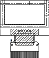
规格图
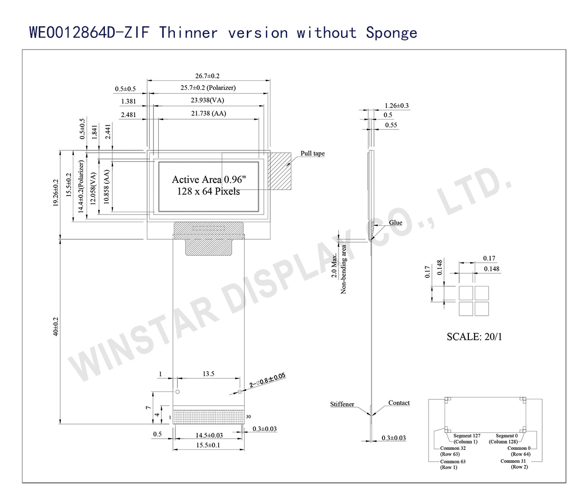
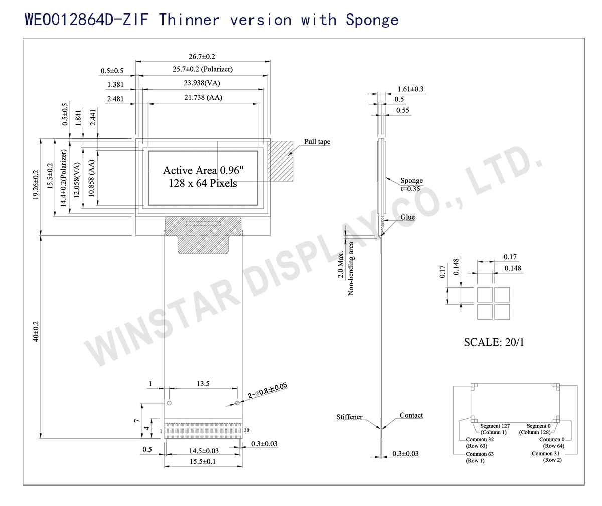
Data source ref: WEO012864DWPP3N00F01
产品规格
Pin功能定义
| No. | 符号 | 功能说明 | ||||||||||||||||||||||||
|---|---|---|---|---|---|---|---|---|---|---|---|---|---|---|---|---|---|---|---|---|---|---|---|---|---|---|
| 1 | N.C. (GND) | Reserved Pin (Supporting Pin) The supporting pins can reduce the influences from stresses on the function pins. These pins must be connected to external ground. |
||||||||||||||||||||||||
| 2 | C2N | Positive Terminal of the Flying Inverting Capacito rNegative Terminal of the Flying Boost Capacitor The charge-pump capacitors are required between the terminals. They must be floated when the converter is not used. | ||||||||||||||||||||||||
| 3 | C2P | |||||||||||||||||||||||||
| 4 | C1P | |||||||||||||||||||||||||
| 5 | C1N | |||||||||||||||||||||||||
| 6 | VBAT | Power Supply for DC/DC Converter Circuit This is the power supply pin for the internal buffer of the DC/DC voltage converter. It must be connected to external source when the converter is used. It should be connected to VDD when the converter is not used. |
||||||||||||||||||||||||
| 7 | NC | NC | ||||||||||||||||||||||||
| 8 | VSS | Ground of Logic Circuit This is a ground pin. It acts as a reference for the logic pins. It must be connected to external ground. |
||||||||||||||||||||||||
| 9 | VDD | Power Supply for Logic This is a voltage supply pin. It must be connected to external source. |
||||||||||||||||||||||||
| 10 | BS0 | Communicating Protocol Select These pins are MCU interface selection input. See the following table:
|
||||||||||||||||||||||||
| 11 | BS1 | |||||||||||||||||||||||||
| 12 | BS2 | |||||||||||||||||||||||||
| 13 | CS# | Chip Select This pin is the chip select input. The chip is enabled for MCU communication only when CS# is pulled low. |
||||||||||||||||||||||||
| 14 | RES# | Power Reset for Controller and Driver This pin is reset signal input. When the pin is low, initialization of the chip is executed. |
||||||||||||||||||||||||
| 15 | D/C# | Data/Command Control This pin is Data/Command control pin. When the pin is pulled high, the input at D7~D0 is treated as display data. When the pin is pulled low, the input at D7~D0 will be transferred to the command register. For detail relationship to MCU interface signals, please refer to the Timing Characteristics Diagrams. When the pin is pulled high and serial interface mode is selected, the data at SDIN is treated as data. When it is pulled low, the data at SDIN will be transferred to the command register. In I2C mode, this pin acts as SA0 for slave address selection. |
||||||||||||||||||||||||
| 16 | R/W# | Read/Write Select or Write This pin is MCU interface input. When interfacing to a 68XX-series microprocessor, this pin will be used as Read/Write (R/W#) selection input. Pull this pin to “High” for read mode and pull it to “Low” for write mode. When 80XX interface mode is selected, this pin will be the Write (WR#) input. Data write operation is initiated when this pin is pulled low and the CS# is pulled low. |
||||||||||||||||||||||||
| 17 | E/RD# | Read/Write Enable or Read This pin is MCU interface input. When interfacing to a 68XX-series microprocessor, this pin will be used as the Enable (E) signal. Read/write operation is initiated when this pin is pulled high and the CS# is pulled low. When connecting to an 80XX-microprocessor, this pin receives the Read (RD#) signal. Data read operation is initiated when this pin is pulled low and CS# is pulled low. |
||||||||||||||||||||||||
| 18~25 | D0~D7 | Host Data Input/Output Bus These pins are 8-bit bi-directional data bus to be connected to the microprocessor’s data bus. When serial mode is selected, D1 will be the serial data input SDIN and D0 will be the serial clock input SCLK. When I2C mode is selected, D2 & D1 should be tired together and serve as SDAout & SDAin in application and D0 is the serial clock input SCL. |
||||||||||||||||||||||||
| 26 | IREF | Current Reference for Brightness Adjustment This pin is segment current reference pin. A resistor should be connected between this pin and VSS. Set the current lower than 12.5μA. |
||||||||||||||||||||||||
| 27 | VCOMH | Voltage Output High Level for COM Signal This pin is the input pin for the voltage output high level for COM signals. A capacitor should be connected between this pin and VSS. |
||||||||||||||||||||||||
| 28 | VCC | Power Supply for OEL Panel This is the most positive voltage supply pin of the chip. A stabilization capacitor should be connected between this pin and VSS when the converter is used. It must be connected to external source when the converter is not used. |
||||||||||||||||||||||||
| 29 | VLSS | Ground of Analog Circuit This is an analog ground pin. It should be connected to VSS externally. |
||||||||||||||||||||||||
| 30 | NC (GND) |
Reserved Pin (Supporting Pin) The supporting pins can reduce the influences from stresses on the function pins. These pins must be connected to external ground. |
规格说明
| 项目 | WEO012864D-ZIF 无Sponge泡棉规格 | WEO012864D-ZIF 有Sponge泡棉规格 | 单位 |
|---|---|---|---|
| 点阵(分辨率) | 128 × 64 | 128 × 64 | Dots |
| 模块尺寸 | 26.70 × 19.26 × 1.26 | 26.70 × 19.26 × 1.61 | mm |
| 有效区域 | 21.738 × 10.858 | 21.738 × 10.858 | mm |
| 像素大小 | 0.148 × 0.148 | 0.148 × 0.148 | mm |
| 像素间距 | 0.17 × 0.17 | 0.17 × 0.17 | mm |
| 显示模式 | 被动矩阵 | 被动矩阵 | |
| 发光颜色 | 单色 | 单色 | |
| 驱动方式 | 1/64 Duty | 1/64 Duty | |
| IC | SSD1306 | SSD1306 | |
| 接口 | 6800,8080,SPI,I2C | 6800,8080,SPI,I2C | |
| 尺寸(对角线) | 0.96 | 0.96 | 寸 |
最大绝对额定值
| 参数 | 符号 | 最小值 | 典型值 | 单位 |
|---|---|---|---|---|
| 逻辑电源电压 | VDD | 0 | 4.0 | V |
| 显示电源电压 | VCC | 0 | 15.0 | V |
| 工作温度 | TOP | -40 | +80 | °C |
| 储存温度 | TSTG | -40 | +85 | °C |
电气特性
| 项目 | 符号 | 条件 | 最小值 | 典型值 | 最大值 | 单位 |
|---|---|---|---|---|---|---|
| 逻辑电源电压 | VDD | - | 2.8 | 3.0 | 3.3 | V |
| 显示电源电压 | VCC | - | 11.5 | 12.0 | 12.5 | V |
| 输入高电压 | VIH | - | 0.8×VDD | - | VDDIO | V |
| 输入低电压 | VIL | - | 0 | - | 0.2×VDD | V |
| 输出高电压 | VOH | - | 0.9×VDD | - | VDDIO | V |
| 输出低电压 | VOL | - | 0 | - | 0.1×VDD | V |
| VDD工作电流 (50% display ON) | ICC | - | - | 19.5 | 25.0 | mA |
FPC options
| Drawing | FPC Length | PIN | Pitch | ZIF FPC or HOTBAR FPC | Interface | FPC No. | Create Date |
|---|---|---|---|---|---|---|---|
 |
22 | 30 | 0.7 | HOTBAR | 6800,8080,SPI,I2C | FPC2070003001XXXXX08 | 20170808 |
 |
41.1 | 30 | 0.5 | ZIF | 6800,8080,SPI,I2C | FPC2050003011XXXXX28 | 20180604 |
 |
13.1 | 30 | 0.5 | ZIF | 6800,8080,SPI,I2C | FPC2050003011XXXXX34 | 20200221 |
")
