


产品叙述
WEO012864C-ZIF是一款ZIF FPC出PIN的COG 绘图型分辨率128x64 的OLED显示器模块。此款WEO012864C-ZIF版与WEO012864C-Hotbar版使用相同的OLED面板,但是采用ZIF FPC出PIN,提供客户更多重选择。此模块对角尺寸仅0.96寸是一款小尺寸超薄型绘图OLED显示器,模块内置SH1106 controller IC支持6800/8080 8-bit 并列接口与 I2C及4线SPI串行接口,1/64 duty驱动。
此模块使用OLED面板低功耗,适用于需要轻薄、小巧、低耗电的产品运用,例如:手持式产品、 量测仪表或仪器、 智能电表、 穿戴装置、 IoT等等。此模块的工作温度是-40℃ 至 +80℃,储存温度为-40℃ 至 +85℃。
规格图
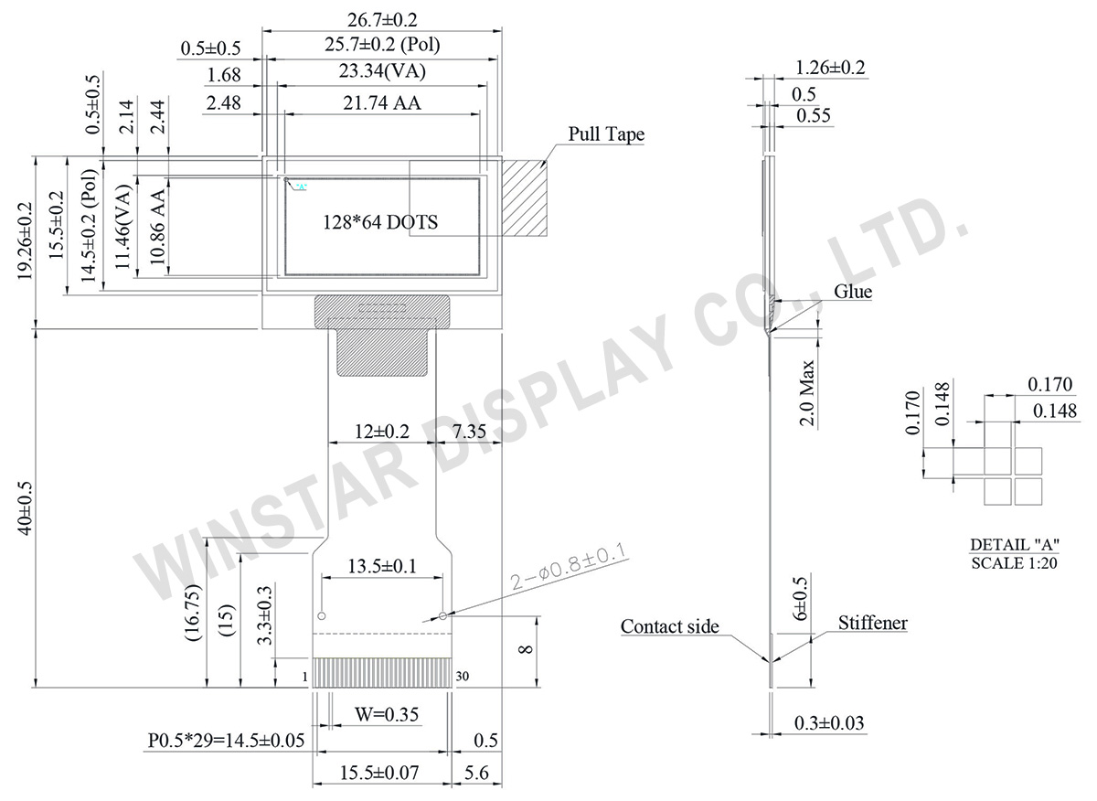
Data source ref: WEO012864CWAP3N00F00
产品规格
Pin功能定义
| No. | 符号 | 功能说明 | ||||||||||||||||||||||||
|---|---|---|---|---|---|---|---|---|---|---|---|---|---|---|---|---|---|---|---|---|---|---|---|---|---|---|
| 1 | NC | No connection | ||||||||||||||||||||||||
| 2 | C1N | Connect to charge pump capacitor. These pins are not used and should be disconnected when Vpp is supplied externally. |
||||||||||||||||||||||||
| 3 | C1P | |||||||||||||||||||||||||
| 4 | C2P | Connect to charge pump capacitor. These pins are not used and should be disconnected when Vpp is supplied externally. |
||||||||||||||||||||||||
| 5 | C2N | |||||||||||||||||||||||||
| 6 | VDD2 | 3.0 – 4.7V power supply pad for Power supply for charge pump circuit. This pin should be disconnected when VPP is supplied externally |
||||||||||||||||||||||||
| 7 | NC | No connection | ||||||||||||||||||||||||
| 8 | VSS | Ground. | ||||||||||||||||||||||||
| 9 | VDD1 | Power supply input: 1.65 - 3.5V | ||||||||||||||||||||||||
| 10 | IM0 | These are the MPU interface mode select pads.
|
||||||||||||||||||||||||
| 11 | IM1 | |||||||||||||||||||||||||
| 12 | IM2 | |||||||||||||||||||||||||
| 13 | CSB | This pad is the chip select input. When CSB = “L”, then the chip select becomes active, and data/command I/O is enabled. | ||||||||||||||||||||||||
| 14 | RESB | This is a reset signal input pad. When RES is set to “L”, the settings are initialized. The reset operation is performed by the RES signal level. | ||||||||||||||||||||||||
| 15 | A0 | This is the Data/Command control pad that determines whether the data bits are data or a command. A0 = “H”: the inputs at D0 to D7 are treated as display data. A0 = “L”: the inputs at D0 to D7 are transferred to the command registers. In I2C interface, this pad serves as SA0 to distinguish the different address of OLED driver. |
||||||||||||||||||||||||
| 16 | WRB | This is a MPU interface input pad. When connected to an 8080 MPU, this is active LOW. This pad connects to the 8080 MPU WR signal. The signals on the data bus are latched at the rising edge of the WR signal. When connected to a 6800 Series MPU: This is the read/write control signal input terminal. When R/W = “H”: Read. When R/W = “L”: Write. |
||||||||||||||||||||||||
| 17 | RDB | This is a MPU interface input pad. When connected to an 8080 series MPU, it is active LOW. This pad is connected to the RD signal of the 8080 series MPU, and the data bus is in an output status when this signal is “L”. When connected to a 6800 series MPU , this is active HIGH. This is used as an enable clock input of the 6800 series MPU. When RD = “H”: Enable. When RD = “L”: Disable. |
||||||||||||||||||||||||
| 18 | D0 | This is an 8-bit bi-directional data bus that connects to an 8-bit or 16-bit standard MPU data bus. When the serial interface is selected, then D0 serves as the serial clock input pad (SCL) and D1 serves as the serial data input pad (SI). At this time, D2 to D7 are set to high impedance. When the I2C interface is selected, then D0 serves as the serial clock input pad (SCL) and D1 serves as the serial data input pad (SDAI). At this time, D2 to D7 are set to high impedance. |
||||||||||||||||||||||||
| 19 | D1 | |||||||||||||||||||||||||
| 20 | D2 | |||||||||||||||||||||||||
| 21 | D3 | |||||||||||||||||||||||||
| 22 | D4 | |||||||||||||||||||||||||
| 23 | D5 | |||||||||||||||||||||||||
| 24 | D6 | |||||||||||||||||||||||||
| 25 | D7 | |||||||||||||||||||||||||
| 26 | IREF | This is a segment current reference pad. A resistor should be connected between this pad and VSS. Set the current at 18.75uA. | ||||||||||||||||||||||||
| 27 | VCOMH | This is a pad for the voltage output high level for common signals. A capacitor should be connected between this pad and VSS. |
||||||||||||||||||||||||
| 28 | VPP | OLED panel power supply. Generated by internal charge pump. Connect to capacitor. It could be supplied externally. |
||||||||||||||||||||||||
| 29 | NC | No connection | ||||||||||||||||||||||||
| 30 | NC | No connection |
规格说明
| 项目 | 规格 | 单位 |
|---|---|---|
| 点阵(分辨率) | 128 x 64 | - |
| 模块尺寸 | 26.70 × 19.26 ×1.26 | mm |
| 有效区域 | 21.74 × 10.86 | mm |
| 点大小 | 0.148 × 0.148 | mm |
| 点间距 | 0.170 × 0.170 | mm |
| 显示模式 | 被动矩阵 | |
| 发光颜色 | 单色 | |
| 驱动方式 | 1/64 Duty | |
| 控制器IC | SH1106 | |
| 接口 | 6800, 8080, SPI, I2C | |
| 尺寸 | 0.96 寸 | |
最大绝对额定值
| 参数 | 符号 | 最小值 | 最大值 | 单位 |
|---|---|---|---|---|
| 逻辑电源电压 | VDD1 | -0.3 | 3.6 | V |
| 电荷帮浦电源 | VDD2 | -0.3 | 4.8 | V |
| 显示电源电压 | VPP | -0.3 | 14.5 | V |
| 工作温度 | TOP | -40 | +80 | °C |
| 储存温度 | TSTG | -40 | +85 | °C |
电气特性
DC 电气特性
| 项目 | 符号 | 条件 | 最小值 | 典型值 | 最大值 | 单位 |
|---|---|---|---|---|---|---|
| 逻辑电源电压 | VDD1 | - | 2.8 | 3.0 | 3.3 | V |
| 电荷帮浦电源 | VDD2 | - | 3.5 | 3.8 | 4.2 | V |
| 显示器的电荷帮浦输出电压 (Generated by Internal DC/DC) |
Charge Pump VPP |
- | 7.5 | 8 | 8.5 | V |
| 输入高准位 | VIH | - | 0.8xVDD1 | - | VDD1 | V |
| 输入低准位 | VIL | - | VSS | - | 0.2xVDD1 | V |
| 输出高准位 | VOH | - | 0.8xVDD1 | - | VDD1 | V |
| 输出低准位 | VOL | - | VSS | - | 0.2xVDD1 | V |
| VDD2的工作电流显示50%ON | IDD2 | - | - | 10 | 16 | mA |
FPC options
| Drawing | FPC Length | PIN | Pitch | ZIF FPC or HOTBAR FPC | Interface | FPC No. | Create Date |
|---|---|---|---|---|---|---|---|
 |
13 | 30 | 0.7 | HOTBAR FPC | 6800, 8080, 4-Wire SPI, I2C | FPC2070003001XXXXX09 | 20180613 |
 |
40.95 | 30 | 0.5 | ZIF | 6800, 8080, SPI, I2C | FPC2050003011XXXXX23 | 20190412 |
Search keyword: 128x64 oled, oled 128x64, 0.96 oled, 0.96" oled, 0.96寸 oled, oled 0.96, oled 0.96"

 - WF70GTIFGDHGV")


