
")
")
")
")
")
")
產品敘述
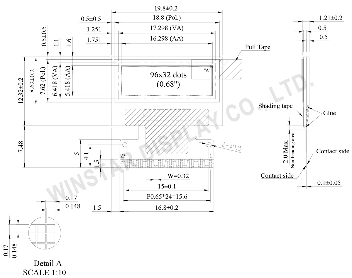
WEO009632B Hotbar版本是一款小型OLED顯示器模組,解析度為96x32像素,尺寸為0.68吋。 模組內建SSD1305驅動器IC; 此模組支援8-bit 6800/8080 並列式介面、 I2C和4線SPI介面。WEO009632B-Hotbar版本電源電壓為3V,驅動為1/32 duty; 50%顯示畫面耗電為6mA@12Vcc (典型值)。OLED顯示器具有超薄、重量輕、低功耗且無需背光等特性。適用於手提式設備、個人護理設備、健康器材、儀表設備…等。WEO009632B-Hotbar模組工作溫度為-40℃至+ 80℃; 儲存溫度為-40℃至+ 85℃。
規格圖
Data source ref: WEO009632BWPP3N00H00
產品規格
Pin功能定義
| Pin No. | 符號 | I/O | 功能 | |||||||||||||||
|---|---|---|---|---|---|---|---|---|---|---|---|---|---|---|---|---|---|---|
| 1 | N.C. | - | Reserved Pin(Supporting Pin) The supporting pins can reduce the influences from stresses on the function pins. These pins must be connected to external ground. |
|||||||||||||||
| 2,23 | VSS | P | Ground of Logic Circuit This is a ground pin. It also acts as a reference for the logic pins. It must be connected to external ground. |
|||||||||||||||
| 3,24 | VCC | P | Power Supply for OLED Panel This is the most positive voltage supply pin of the chip. It must be supplied externally. |
|||||||||||||||
| 4 | VCOMH | O | Voltage Output High Level for COM Signal This pin is the input pin for the voltage output high level for COM signals. A capacitor should be connected between this pin and VSS. |
|||||||||||||||
| 5 | IREF | I | Current Reference for Brightness Adjustment This pin is segment current reference pin. A resistor should be connected between this pin and VSS. Set the current lower than 10μA. |
|||||||||||||||
| 6 | D0~D7 | I/O | Host Data In put/ Output Bus These pins are 8-bit bi-directional data bus to be connected to the microprocessor’s data bus. When serial mode is selected, D1 will be the serial data input SDIN and D0 will be the serial clock input SCLK. When I2Cmode is selected, D2 & D1 should be tired together and serve as SDAout & SDAin in application and D0 is the serial clock input SCL. |
|||||||||||||||
| 7 | ||||||||||||||||||
| 8 | ||||||||||||||||||
| 9 | ||||||||||||||||||
| 10 | ||||||||||||||||||
| 11 | ||||||||||||||||||
| 12 | ||||||||||||||||||
| 13 | ||||||||||||||||||
| 14 | E(RD#) | I | Read/Write Enable or Read This pin is MCU interface input. When interfacing to a68XX-series microprocessor, this pin will be used as the Enable (E) signal. Read/write operation is initiated when this pin is pulled high and the CS# is pulled low. When connecting to an 80XX-microprocessor, this pin receives the Read (RD#) signal. Data read operation is initiated when this pin is pulled low and CS# is pulled low. |
|||||||||||||||
| 15 | R/W# (WR#) |
I | Read/ Write Selector Write This pin is MCU interface input. When interfacing to a68XX-series microprocessor, this pin will be used as Read/Write (R/W#) selection input. Pull this pin to “High” for read mode and pull it to “Low” for write mode. When 80XXinterface mode is selected, this pin will be the Write (WR#) input. Data write operation is initiated when this pin is pulled low and the CS# is pulled low. |
|||||||||||||||
| 16 | D/C# | I | Data/ Command Control This pin is Data/Command control pin. When the pin is pulled high, the input at D7~D0 is treated as display data. When the pin is pulled low, the input at D7~D0 will be transferred to the command register. For detail relationship to MCU interface signals, please refer to the Timing Characteristics Diagrams. When the pin is pulled high and serial interface mode is selected, the data at SDIN is treated as data. When it is pulled low, the data at SDIN will be transferred to the command register. In I2C mode, this pin acts as SA0 for slave address selection. |
|||||||||||||||
| 17 | RES# | I | Power Reset for Controller and Driver This pin is reset signal input. When the pin is low, initialization of the chip is executed. |
|||||||||||||||
| 18 | CS# | I | Chip Select This pin is the chip select input. The chip is enabled for MCU communication only when CS# is pulled low. |
|||||||||||||||
| 19 | BS2 | I | Communicating Protocol Select These pins are MCU interface selection input. See the following table:
(1) 0 is connected to VSS (2) 1 is connected to VDDIO |
|||||||||||||||
| 20 | BS1 | I | ||||||||||||||||
| 21 | VDDIO | P | Power supply for interface logic level. It should be match with MCU interface voltage level. VDDIO must always be equal or lower than VDD. |
|||||||||||||||
| 22 | VDD | P | Power Supply for Logic Circuit This is a voltage supply pin. It must be connected to external source. |
|||||||||||||||
| 25 | N.C. | - | Reserved Pin(Supporting Pin) The supporting pins can reduce the influences from stresses on the function pins. These pins must be connected to external ground. |
規格說明
| 項目 | 規格 | 單位 |
|---|---|---|
| 解析度 | 96 × 32 | Dots |
| 模組尺寸 | 19.80 × 12.32 × 1.21 (mm) | mm |
| 有效區域 | 16.298 × 5.418 (mm) | mm |
| 像素大小 | 0.148 × 0.148 (mm) | mm |
| 像素間距 | 0.17 × 0.17 (mm) | mm |
| 顯示模式 | 被動矩陣 | |
| 發光顏色 | 單色 | |
| 驅動方式 | 1/32 Duty | |
| IC | SSD1305 | |
| 介面 | 6800, 8080, SPI, I2C | |
| 尺寸 | 0.68 吋 | |
最大絕對額定值
| 參數 | 符號 | 最小值 | 最大值 | 單位 |
|---|---|---|---|---|
| 邏輯電源電壓 | VDD | -0.3 | 4 | V |
| 顯示電源電壓 | VCC | 0 | 16 | V |
| 工作溫度 | TOP | -40 | +80 | °C |
| 儲存溫度 | TSTG | -40 | +85 | °C |
電氣特性
DC特性
| 項目 | 符號 | 條件 | 最小值 | 典型值 | 最大值 | 單位 |
|---|---|---|---|---|---|---|
| 邏輯電源電壓 | VDD | - | 2.8 | 3.0 | 3.3 | V |
| 顯示電源電壓 | VCC | - | 11.5 | 12 | 12.5 | V |
| 輸入高準位 | VIH | - | 0.8×VDD | - | VDD | V |
| 輸入低準位 | VIL | - | 0 | - | 0.2×VDD | V |
| 輸出高準位 | VOH | Iout = 100uA | 0.9×VDD | - | VDD | V |
| 輸出低準位 | VOL | Iout = 100uA | 0 | - | 0.1×VDD | V |
| 符號 | 參數 | 最小值 | 典型值 | 最大值 | 單位 | 條件 |
|---|---|---|---|---|---|---|
| ICC | VCC Supply Current | - | 6 | 9 | mA | VDD =3.0V , Display 100% ON |
FPC options
| Drawing | FPC Length | PIN | pitch | ZIF FPC or HOTBAR FPC | Interface | FPC No. | Create Date |
|---|---|---|---|---|---|---|---|
 |
30 | 28 | 0.5 | ZIF FPC | 6800, 8080,4-Wire SPI, I2C | FPC2050002811XXXXX01 | 20180131 |
 |
8.479 | 25 | 0.65 | HOTBAR FPC | 6800, 8080,4-Wire SPI, I2C | FPC2065002501XXXXX00 | 20190906 |
Search keyword: 96x32 oled, oled 96x32, 0.68 oled, 0.68" oled, 0.68吋 oled, oled 0.68, oled 0.68"
