


產品敘述
WEX025664B-CTP是一款3.12吋COF結構繪圖型OLED顯示器,解析度由256x64 dots所組成,模組上帶有電容式觸控玻璃。 此OLED模組使用COF SSD1322 IC可以透過6800 / 8080 8-bit並列介面或SPI串列介面進行通信,支援4-bits灰階。模組邏輯電源電壓為2.8V至3.3V;Typical值為3V;顯示電源電壓為14.5V,1/64 driving duty。 WEX025664B-CTP OLED模組其觸控面板IC使用FT6336U並支援I2C介面和單指觸控。 請注意,此款型號可以選配含鐵框的模組,細節歡迎來信詢問。
此款帶有CTP型號的3.12" WEX025664B-CTP非常適用於智能家居應用、智能技術設備、儀表設備、工業控制系統、醫療儀器等。模組的工作溫度為-20℃至+70℃;儲存溫度範圍為-30℃至+80℃。
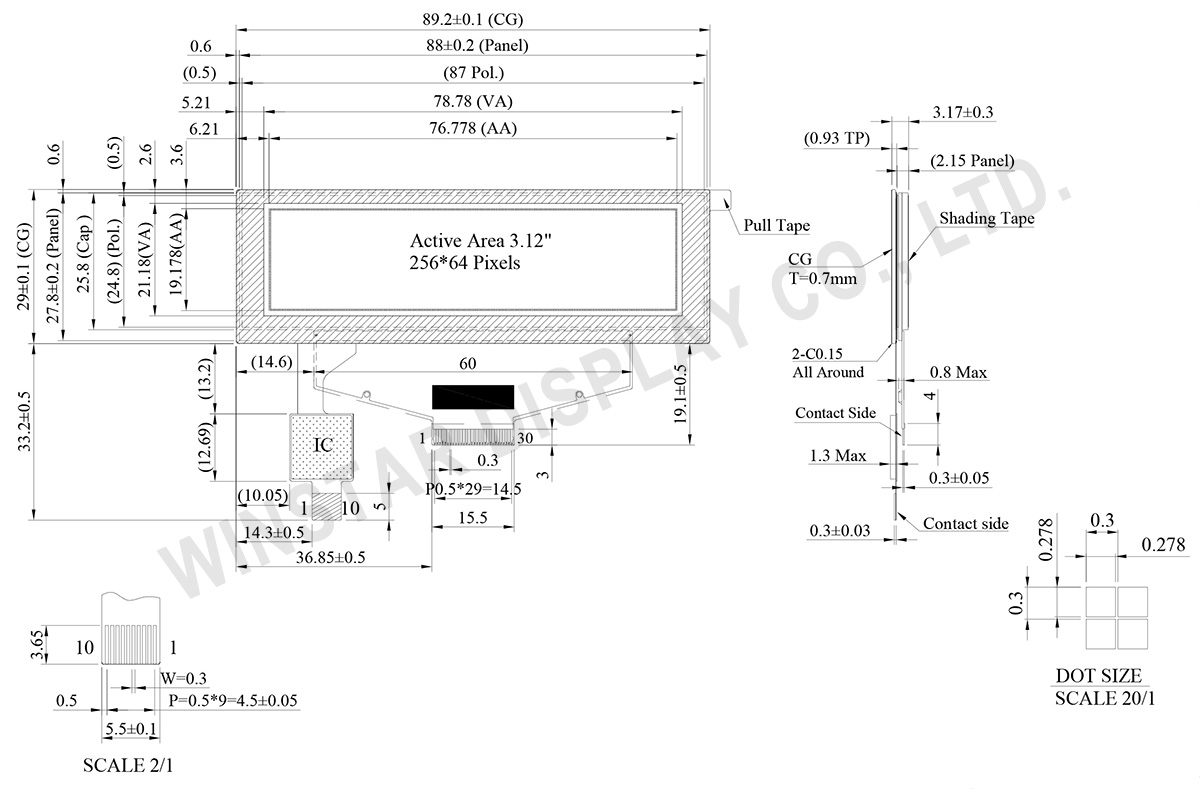
規格圖
Data source ref: WEX025664BWPP3D00000
產品規格
Pin功能定義
| No. | 符號 | 功能說明 | ||||||||||
|---|---|---|---|---|---|---|---|---|---|---|---|---|
| 1 | N.C. | Reserved Pin The N.C. pin between function pins are reserved for compatible and flexible design. |
||||||||||
| 2 | VSS | Ground. | ||||||||||
| 3 | VCC | Power supply for panel driving voltage. This is also the most positive power voltage supply pin. |
||||||||||
| 4 | VCOMH | COM signal deselected voltage level. A capacitor should be connected between this pin and VSS. |
||||||||||
| 5 | VLSS | Analog system ground pin. | ||||||||||
| 6~13 | D7~D0 | Host Data Input/Output Bus These pins are 8-bit bi-directional data bus to be connected to the microprocessor’s data bus. When serial mode is selected, D1 will be the serial data input SDIN and D0 will be the serial clock input SCLK. |
||||||||||
| 14 | E/RD# | Read/Write Enable or Read This pin is MCU interface input. When interfacing to a 68XX-series microprocessor, this pin will be used as the Enable (E) signal. Read/write operation is initiated when this pin is pulled high and the CS# is pulled low. When connecting to an 80XX-microprocessor, this pin receives the Read (RD#) signal. Data read operation is initiated when this pin is pulled low and CS# is pulled low. When serial mode is selected, this pin must be connected to VSS. |
||||||||||
| 15 | R/W# | Read/Write Select or Write This pin is MCU interface input. When interfacing to a 68XX-series microprocessor, this pin will be used as Read/Write (R/W#) selection input. Pull this pin to “High” for read mode and pull it to “Low” for write mode. When 80XX interface mode is selected, this pin will be the Write (WR#) input. Data write operation is initiated when this pin is pulled low and the CS# is pulled low. When serial mode is selected, this pin must be connected to VSS. |
||||||||||
| 16 | BS0 | Communicating Protocol Select These pins are MCU interface selection input. See the following table:
(1) 0 is connected to VSS (2) 1 is connected to VDDIO |
||||||||||
| 17 | BS1 | |||||||||||
| 18 | D/C# | Data/Command Control This pin is Data/Command control pin connecting to the MCU. When the pin is pulled HIGH, the content at D[7:0] will be interpreted as data. When the pin is pulled LOW, the content at D[7:0] will be interpreted as command. |
||||||||||
| 19 | CS# | Data/Command Control This pin is the chip select input connecting to the MCU. The chip is enabled for MCU communication only when CS# is pulled LOW. |
||||||||||
| 20 | RES# | This pin is reset signal input. When the pin is pulled LOW, initialization of the chip is executed. Keep this pin pull HIGH during normal operation. |
||||||||||
| 21 | FR | This pin is No Connection pins. Nothing should be connected to this pin. This pin should be left open individually. | ||||||||||
| 22 | IREF | Current Reference for Brightness Adjustment This pin is segment current reference pin. A resistor should be connected between this pin and VSS. Set the current lower than 10uA. |
||||||||||
| 23 | N.C. | Reserved Pin The N.C. pin between function pins are reserved for compatible and flexible design. |
||||||||||
| 24 | VDDIO | Power Supply for I/O Pin It should be matched with the MCU interface voltage level. |
||||||||||
| 25 | VDD | Power Supply for Core Logic Circuit Power supply pin for core logic operation. A capacitor is required to connect between this pin and VSS |
||||||||||
| 26 | VCI | Power Supply for Operation VCI must always be equal to or higher than VDD and VDDIO. |
||||||||||
| 27 | VSL | Voltage Output Low Level for SEG Signal This is segment voltage reference pin. When external VSL is not used, this pin should be left open. When external VSL is used, this pin should connect with resistor and diode to ground. |
||||||||||
| 28 | VLSS | Ground of Analog Circuit These are the analog ground pins. They should be connected to VSS externally. |
||||||||||
| 29 | VCC | Power Supply for OLED Panel These are the most positive voltage supply pin of the chip. They must be connected to external source. |
||||||||||
| 30 | N.C. | Reserved Pin The N.C. pin between function pins are reserved for compatible and flexible design. |
CTP 功能定義
| 1 | GND | Ground |
| 2 | VDD | Power Supply Voltage of CTP |
| 3 | INT | External interrupt to the host |
| 4 | SDA | I2C data input and output |
| 5 | SCL | I2C clock input |
| 6 | RST | External Reset, Low is active |
| 7-10 | GND | Ground. |
規格說明
| 項目 | 尺寸 | 單位 |
|---|---|---|
| 點陣 | 256 x 64 Dots | - |
| 模組尺寸 | 89.2 × 29.0 × 3.17 | mm |
| 有效區域 | 76.778×19.178 | mm |
| 點大小 | 0.278×0.278 | mm |
| 點間距 | 0.3×0.3 | mm |
| 顯示模式 | 被動矩陣 | |
| 發光顏色 | 單色 | |
| 驅動方式 | 1/64 Duty | |
| 灰階 | 4 bits | |
| OLED IC | SSD1322 (COF) | |
| OLED 介面 | 6800, 8080, SPI | |
| 尺寸(對角線) | 3.12 吋 | |
| CTP IC | FT6336U | |
| 支援手指數 | 1 | |
| CTP 介面 | I2C | |
| 表面 | 亮面 | |
最大絕對額定值
最大絕對額定值
| 參數 | 符號 | 最小值 | 最大值 | 單位 |
|---|---|---|---|---|
| 工作電源電壓 | VCI | -0.3 | 4 | V |
| 邏輯電源電壓 | VDD | -0.5 | 2.75 | V |
| I/O pin 供電電壓 | VDDIO | -0.5 | VCI | V |
| 顯示電源電壓 | VCC | -0.5 | 20 | V |
| 工作溫度 | TOP | -20 | +70 | °C |
| 儲存溫度 | TSTG | -30 | +80 | °C |
觸控面板控制器 FT6336U
| 參數 | 符號 | 最小值 | 最大值 | 單位 |
|---|---|---|---|---|
| 電源電壓 | VDD | -0.3 | 3.6 | V |
電氣特性
DC 電氣特性
| 項目 | 符號 | 條件 | 最小值 | 典型值 | 最大值 | 單位 |
|---|---|---|---|---|---|---|
| 工作電源電壓 | VCI | Note | 2.8 | 3.0 | 3.3 | V |
| 顯示電源電壓 | VCC | - | 14 | 14.5 | 15 | V |
| 邏輯電源電壓 | VDD | - | 2.4 | - | 2.6 | V |
| I/O Pin 電源 | VDDIO | - | 1.65 | VCI | V | |
| 輸入高準位 | VIH | - | 0.8×VDDIO | - | VDDIO | V |
| 輸入低準位 | VIL | - | 0 | - | 0.2×VDDIO | V |
| 輸出高準位 | VOH | - | 0.9×VDDIO | - | VDDIO | V |
| 輸出低準位 | VOL | - | 0 | - | 0.1×VDDIO | V |
| 50%顯示畫面耗電流 | VCC =14.5V | - | 32 | 48 | mA | |
觸控面板控制器 FT6336U
| 項目 | 符號 | 條件 | 最小值 | 典型值 | 最大值 | 單位 |
|---|---|---|---|---|---|---|
| 電源電壓 | VDD | 2.8 | 3.0 | 3.3 | V | |
| 輸入高準位 | VIH | 0.7xVDD | - | VDD | V | |
| 輸入低準位 | VIL | -0.3 | - | 0.3xVDD | V | |
| 輸出高準位 | VOH | IOH = -0.1mA | 0.7xVDD | - | - | V |
| 輸出低準位 | VOL | IOH = 0.1mA | - | - | 0.3xVDD | V |
Search keyword: 256x64 oled, oled 256x64, 3.12 oled, 3.12" oled, 3.12吋oled, oled 3.12"
