


產品敘述
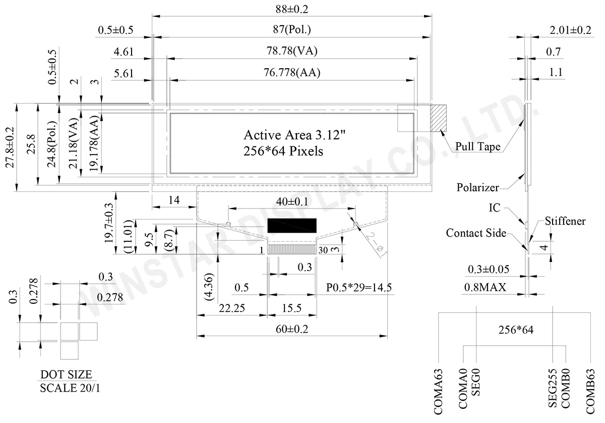
WEX025664B為3.12吋OLED COF 繪圖型標準品。此OLED 顯示器 256x64為不含鐵框模組,內建SSD1322驅動IC,外觀尺寸為 88 x 27.8 mm, AA尺寸為76.778 x 19.178 mm。Winstar COF OLED模組系列非常適合牆面型(wall devices) 與測量儀器(meter devices),例如POS系統、雲端/物聯網系統、手持式產品、智能科技與智慧能源系統、車載與通訊設備以及醫療儀器等等,客戶能便利地將原來產品上的STN顯示器輕易地升級到OLED顯示器,因為華凌光電提供非常多樣化與廣度的OLED尺寸與OLED產品提升解決方案供客戶產品升級。
規格圖
產品規格
Pin功能定義
| Pin Number | 符號 | I/O | 功能說明 | ||||||||||
|---|---|---|---|---|---|---|---|---|---|---|---|---|---|
| 1 | N.C. (GND) | P | Ground | ||||||||||
| 2 | VSS | P | Ground. | ||||||||||
| 3 | VCC | P | Power supply for panel driving voltage. This is also the most positive power voltage supply pin. |
||||||||||
| 4 | VCOMH | P | COM signal deselected voltage level. A capacitor should be connected between this pin and VSS. |
||||||||||
| 5 | VLSS | P | Analog system ground pin. | ||||||||||
| 6~13 | D7~D0 | I/O | Host Data Input/Output Bus These pins are 8-bit bi-directional data bus to be connected to the microprocessor’s data bus. When serial mode is selected, D1 will be the serial data input SDIN and D0 will be the serial clock input SCLK. |
||||||||||
| 14 | E/RD# | I | Read/Write Enable or Read This pin is MCU interface input. When interfacing to a 68XX-series microprocessor, this pin will be used as the Enable (E) signal. Read/write operation is initiated when this pin is pulled high and the CS# is pulled low. When connecting to an 80XX-microprocessor, this pin receives the Read (RD#) signal. Data read operation is initiated when this pin is pulled low and CS# is pulled low. When serial mode is selected, this pin must be connected to VSS. |
||||||||||
| 15 | R/W# | I | Read/Write Select or Write This pin is MCU interface input. When interfacing to a 68XX-series microprocessor, this pin will be used as Read/Write (R/W#) selection input. Pull this pin to “High” for read mode and pull it to “Low” for write mode. When 80XX interface mode is selected, this pin will be the Write (WR#) input. Data write operation is initiated when this pin is pulled low and the CS# is pulled low. When serial mode is selected, this pin must be connected to VSS. |
||||||||||
| 16 | BS0 | I | Communicating Protocol Select These pins are MCU interface selection input. See the following table:
(1) 0 is connected to VSS (2) 1 is connected to VDDIO |
||||||||||
| 17 | BS1 | ||||||||||||
| 18 | D/C# | I | Data/Command Control This pin is Data/Command control pin connecting to the MCU. When the pin is pulled HIGH, the content at D[7:0] will be interpreted as data. When the pin is pulled LOW, the content at D[7:0] will be interpreted as command. |
||||||||||
| 19 | CS# | I | Data/Command Control This pin is the chip select input connecting to the MCU. The chip is enabled for MCU communication only when CS# is pulled LOW. |
||||||||||
| 20 | RES# | I | This pin is reset signal input. When the pin is pulled LOW, initialization of the chip is executed. Keep this pin pull HIGH during normal operation. |
||||||||||
| 21 | FR | O | This pin is No Connection pins. Nothing should be connected to this pin. This pin should be left open individually. | ||||||||||
| 22 | IREF | I | Current Reference for Brightness Adjustment This pin is segment current reference pin. A resistor should be connected between this pin and VSS. Set the current lower than 10uA. |
||||||||||
| 23 | N.C. | - | Reserved Pin The N.C. pin between function pins are reserved for compatible and flexible design. |
||||||||||
| 24 | VDDIO | P | Power Supply for I/O Pin It should be matched with the MCU interface voltage level. |
||||||||||
| 25 | VDD | P | Power Supply for Core Logic Circuit Power supply pin for core logic operation. A capacitor is required to connect between this pin and VSS |
||||||||||
| 26 | VCI | P | Power Supply for Operation VCI must always be equal to or higher than VDD and VDDIO. |
||||||||||
| 27 | VSL | P | Voltage Output Low Level for SEG Signal This is segment voltage reference pin. When external VSL is not used, this pin should be left open. When external VSL is used, this pin should connect with resistor and diode to ground. |
||||||||||
| 28 | VLSS | P | Ground of Analog Circuit These are the analog ground pins. They should be connected to VSS externally. |
||||||||||
| 29 | VCC | P | Power Supply for OLED Panel These are the most positive voltage supply pin of the chip. They must be connected to external source. |
||||||||||
| 30 | N.C. (GND) | P | Ground |
規格說明
| 項目 | 尺寸 | 單位 |
|---|---|---|
| 點陣 | 256 x 64 Dots | - |
| 模組尺寸 | 88.0 × 27.8 × 2.01 | mm |
| 有效區域 | 76.778×19.178 | mm |
| 像素大小 | 0.278×0.278 | mm |
| 像素間距 | 0.3×0.3 | mm |
| 顯示模式 | 被動矩陣 | |
| 發光顏色 | 單色 | |
| 驅動方式 | 1/64 Duty | |
| 灰階 | 4 bits | |
| IC | SSD1322 (COF) | |
| 介面 | 6800, 8080, SPI | |
| 尺寸 | 3.12 吋 | |
最大絕對額定
| 參數 | 符號 | 最小值 | 最大值 | 單位 |
|---|---|---|---|---|
| 工作電源電壓 | VCI | -0.3 | 4 | V |
| 邏輯電源電壓 | VDD | -0.5 | 2.75 | V |
| I/O pin 供電電壓 | VDDIO | -0.5 | VCI | V |
| 顯示電源電壓 | VCC | -0.5 | 20 | V |
| 工作溫度 | TOP | -40 | 80 | °C |
| 儲存溫度 | TSTG | -40 | 85 | °C |
電氣特性
| 項目 | 符號 | 條件 | 最小值 | 典型值 | 最大值 | 單位 |
|---|---|---|---|---|---|---|
| 邏輯電源電壓 | VDD | - | 2.4 | 2.5 | 2.6 | V |
| I/O Pin 電源 | VDDIO | - | 1.65 | 3.0 | VCI | V |
| 低壓電源 | VCI | - | 2.4 | 3.0 | 3.5 | V |
| 顯示電源電壓 | VCC | - | 11.5 | 14.5 | 15 | V |
| 輸入高準位 | VIH | - | 0.8×VDDIO | - | VDDIO | V |
| 輸入低準位 | VIL | - | 0 | - | 0.2×VDDIO | V |
| 輸出高準位 | VOH | - | 0.9×VDDIO | - | VDDIO | V |
| 輸出低準位 | VOL | - | 0 | - | 0.1×VDDIO | V |
| 50%顯示畫面耗電流 | ICC | VCC =12V | - | 24 | 32 | mA |
| VCC =14.5V | - | 32 | 42.5 | mA |
Search keyword: 256x64 oled, oled 256x64, 3.12 oled, 3.12" oled, 3.12 inch oled, oled 3.12, oled 3.12", 3.12吋oled


