


Pantalla TFT LVDS 10 pulgadas
Modelo Nº WF104FTIAMLNN0
►Pantalla 10 pulgadas
►Resolución : 1024×768 puntos
►Interfaz : LVDS
►Controlador integrado : --
►Placa de control : No
►Brillo (cd/m²) : 350
►Agujero del bastidor : No
►Pantalla táctil : Sin panel táctil
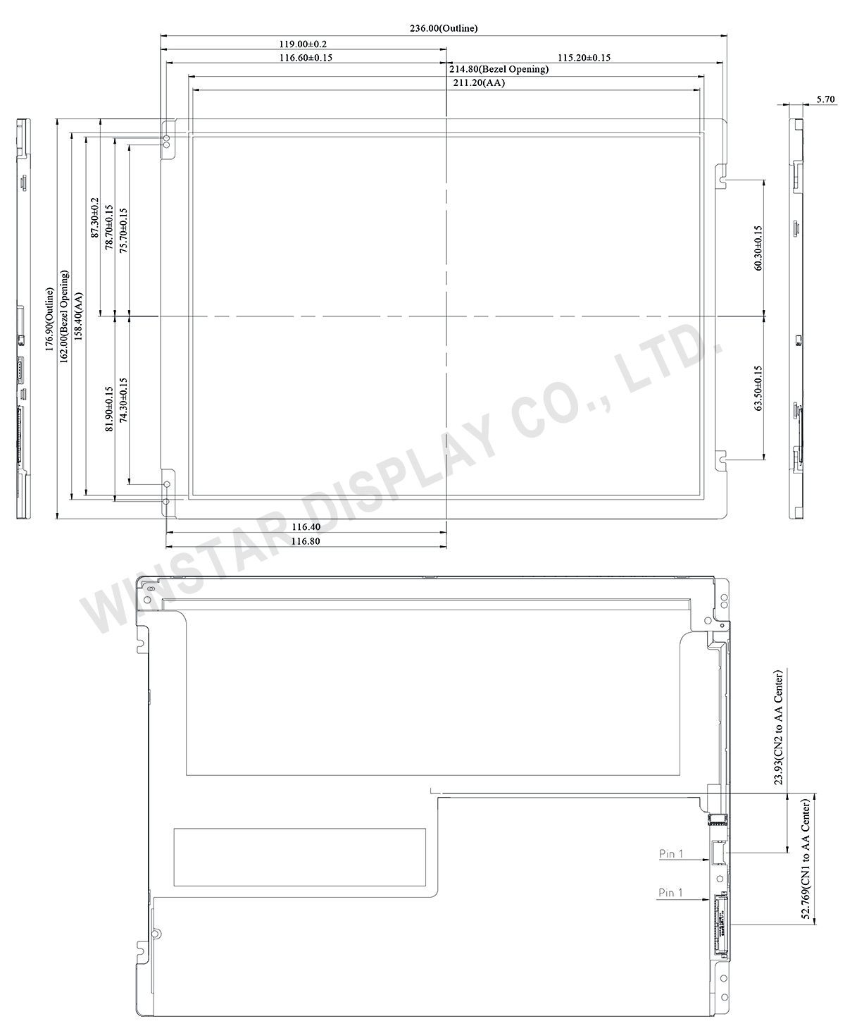
DIBUJO
ESPECIFICACIONES
Función interfaz Pin
Signal Connector Type
| Elemento | Descripción |
|---|---|
| Type / Part Number | MSB24013P20HA (Manufacture by STM) |
| Mating Receptacle / Type (Reference) | P24013P20 or compatible |
Signal Connector Pin Assignment
| Pin No. | Símbolo | Function |
|---|---|---|
| 1 | VDD | Power Supply, 3.3V (typical) |
| 2 | VDD | Power Supply, 3.3V (typical) |
| 3 | VSS | Ground |
| 4 | REV | Reverse Scan selection {High:2.5(min), 3.3(typ),3.6(max); Low: 0.5(max)} |
| 5 | Rin1- | -LVDS differential data input (R0-R5,G0) |
| 6 | Rin1+ | +LVDS differential data input (R0-R5,G0) |
| 7 | VSS | Ground |
| 8 | Rin2- | -LVDS differential data input (G1-G5,B0-B1) |
| 9 | Rin2+ | +LVDS differential data input (G1-G5,B0-B1) |
| 10 | VSS | Ground |
| 11 | Rin3- | -LVDS differential data input (B2-B5,HS,VS,DE) |
| 12 | Rin3+ | +LVDS differential data input (B2-B5,HS,VS,DE) |
| 13 | VSS | Ground |
| 14 | CIkIN- | -LVDS differential clock input |
| 15 | CIkIN+ | +LVDS differential clock input |
| 16 | GND | Ground |
| 17 | Rin4- | -LVDS differential data input (R6-R7,G6-G7,B6-B7) |
| 18 | Rin4+ | +VDS differential data input (R6-R7,G6-G7,B6-B7) |
| 19 | SEL68 | 6/8 bits LVDS data input selection(H:8bits L/NC:6bits) |
| 20 | Bist | Internal use |
Especificaciones generales
| Elemento | Dimensión | Unidad |
|---|---|---|
| Tamaño | 10.4 | pulgada |
| Matriz de puntos | 1024×R.G.B.×768 | dots |
| Dimensión del módulo | 236.0×176.9×5.7 | mm |
| zona activa | 211.2×158.4 | mm |
| Distancia entre puntos | 0.20625×0.20625 | mm |
| Tipo de LCD | TFT, Blanco, Transmisivo | |
| Dirección de inversión de escala de grises | 6 o'clock | |
| Tipo de retroiluminación | LED, Blanco | |
| Interfaz | LVDS | |
| Con o sin panel táctil | Sin panel táctil | |
| Superficie | Pantalla antirreflectante | |
Valores nominales máximos absolutos
| Elemento | Símbolo | Valor mín. | Valor típico | Valor máx. | Unidad |
|---|---|---|---|---|---|
| Temperatura de funcionamiento | TOP | -20 | - | +70 | ℃ |
| Temperatura de almacenamiento | TST | -30 | - | +80 | ℃ |
Características electrónicas
| Elemento | Símbolo | Valor mín. | Valor típico | Valor máx. | Unidad | |
|---|---|---|---|---|---|---|
| LCD Drive Voltage (Logic) | VDD | 3.0 | 3.3 | 3.6 | V | |
| VDD Current | Black Pattern | IDD | - | TBD | (0.25) | A |
| VDD Power Consumption | Black Pattern | PDD | - | - | (0.84) | W |
| Rush Current | Irush | - | - | 1.5 | A | |
| Allowable Logic/LCD Drive Ripple Voltage | VDDrp | - | - | (200) | mV | |

