


Олед дисплей 1.92", 160x128
№ модели WEO160128A
►Тип: Графический
►Тип монтажа контроллера: COG
►Диагональ: 1.92 дюйма
►Разрешение: 160 x 128 точек
►Встроенный контроллер SH1108
►3V Power supply
►1/128 duty
►Интерфейс: 6800, 8080, SPI, I2C
►Цвет дисплея: Белый / Желтый
Описание
WEO0160128A – это новый 1.92' дюймовый COG PMOLED дисплей c разрешением 160x128 точек. Модуль сделан на базе контроллера IC SH1108 c поддержкой интерфейсов: параллельного 6800/8080 8-Бит, I2C и четырехжильного SPI интерфейса. Напряжение питания 3V, напряжение питания для логики дисплея 12V, а рабочий цикл 1/128.
Данный индикатор идеально подходит для применения в: настенных измерительных приборах, измерительных приборах промышленного применения, POS системах, Облачных/IoT системах, умных устройствах, автомобилестроении, коммуникационных системах, медицинских устройствах и т.д.
WEO0160128A может работать при температурах от -40 ° С до + 80 ℃; а температура хранения - от -40 ℃ до + 85 ℃. В настоящее время индикатор доступен в белом цвете; другие цвета находятся в стадии разработки и будут скоро доступны. Ниже приведена основная спецификация:
DRAWING
Data source ref: WEO160128AWPP3N00000
Техническое описание
Функции контроллера контактного интерфейса
| No. | Символы | Описание | ||||||||||||||||||||||||
|---|---|---|---|---|---|---|---|---|---|---|---|---|---|---|---|---|---|---|---|---|---|---|---|---|---|---|
| 1 | NC | No connection | ||||||||||||||||||||||||
| 2 | VPP | This is the most positive voltage supply pad of the chip. It should be supplied externally. |
||||||||||||||||||||||||
| 3 | VSEGM | This is a pad for the voltage output level for segment pre-charge. A capacitor should be connected between this pad and VSS. |
||||||||||||||||||||||||
| 4 | VCOMH | This is a pad for the voltage output high level for common signals. A capacitor should be connected between this pad and VSS. |
||||||||||||||||||||||||
| 5 | VSL | This is a segment voltage reference pad. A capacitor should be connected between this pad and VSS. |
||||||||||||||||||||||||
| 6 | NC | No connection | ||||||||||||||||||||||||
| 7 | IREF | This is a segment current reference pad. A resistor should be connected between this pad and VSS. Set the current at 15.625uA. |
||||||||||||||||||||||||
| 8 | VPP | This is the most positive voltage supply pad of the chip. It should be supplied externally. |
||||||||||||||||||||||||
| 9 | NC | No connection | ||||||||||||||||||||||||
| 10 | VSS | Ground for analog, logic & buffer respectively. | ||||||||||||||||||||||||
| 11 | VCL | This is a common voltage reference pad. This pad should be connected to VSS externally. |
||||||||||||||||||||||||
| 12 | VDD | 1.65 - 3.5V power supply input pad for logic. | ||||||||||||||||||||||||
| 13 | IM0 | These are the MPU interface mode select pads.
|
||||||||||||||||||||||||
| 14 | IM1 | |||||||||||||||||||||||||
| 16 | IM2 | |||||||||||||||||||||||||
| 15 | VDD | 1.65 - 3.5Vpower supply input pad | ||||||||||||||||||||||||
| 17 | CS | This pad is the chip select input. When CS = “L”, then the chip select becomes active, and data command I/O is enabled. | ||||||||||||||||||||||||
| 18 | RES | This is a reset signal input pad. When RES is set to “L”, the settings are initialized. The reset operation is performed by the RES signal level. | ||||||||||||||||||||||||
| 19 | A0 | This is the Data/Command control pad that determines whether the data bits are data or a command. A0 = “H”: the inputs at D0 to D7 are treated as display data. A0 = “L”: the inputs at D0 to D7 are transferred to the command registers. In I2C interface, this pad serves as SA0 to distinguish the different address of OLED driver. |
||||||||||||||||||||||||
| 20 | WR | This is a MPU interface input pad. When connected to an 8080 MPU, this is active LOW. This pad connects to the 8080 MPU WR signal. The signals on the data bus are latched at the rising edge of the WR signal. When connected to a 6800 Series MPU: This is the read/write control signal input terminal. When WR = “H”: Read. When WR = “L”: Write. |
||||||||||||||||||||||||
| 21 | RD | This is a MPU interface input pad. When connected to an 8080 series MPU, it is active LOW. This pad is connected to the RD signal of the 8080 series MPU, and the data bus is in an output status when this signal is “L”. When connected to a 6800 series MPU, this is active HIGH. This is used as an enable clock input of the 6800 series MPU. |
||||||||||||||||||||||||
| 22 | D0 | This is an 8-bit bi-directional data bus that connects to an 8-bit or 16-bit standard MPU data bus. When the serial interface is selected, then D0 serves as the serial clock input pad (SCL) and D1 serves as the serial data input pad (SI). At this time, D2 to D7 are set to high impedance. When the I2C interface is selected, then D0 serves as the serial clock input pad (SCL) and D1 serves as the serial data input pad (SDA). At this time, D2 to D7 are set to high impedance. |
||||||||||||||||||||||||
| 23 | D1 | |||||||||||||||||||||||||
| 24 | D2 | |||||||||||||||||||||||||
| 25 | D3 | |||||||||||||||||||||||||
| 26 | D4 | |||||||||||||||||||||||||
| 27 | D5 | |||||||||||||||||||||||||
| 28 | D6 | |||||||||||||||||||||||||
| 29 | D7 | |||||||||||||||||||||||||
| 30 | NC | No connection | ||||||||||||||||||||||||
| 31 | VPP | This is the most positive voltage supply pad of the chip. It should be supplied externally. |
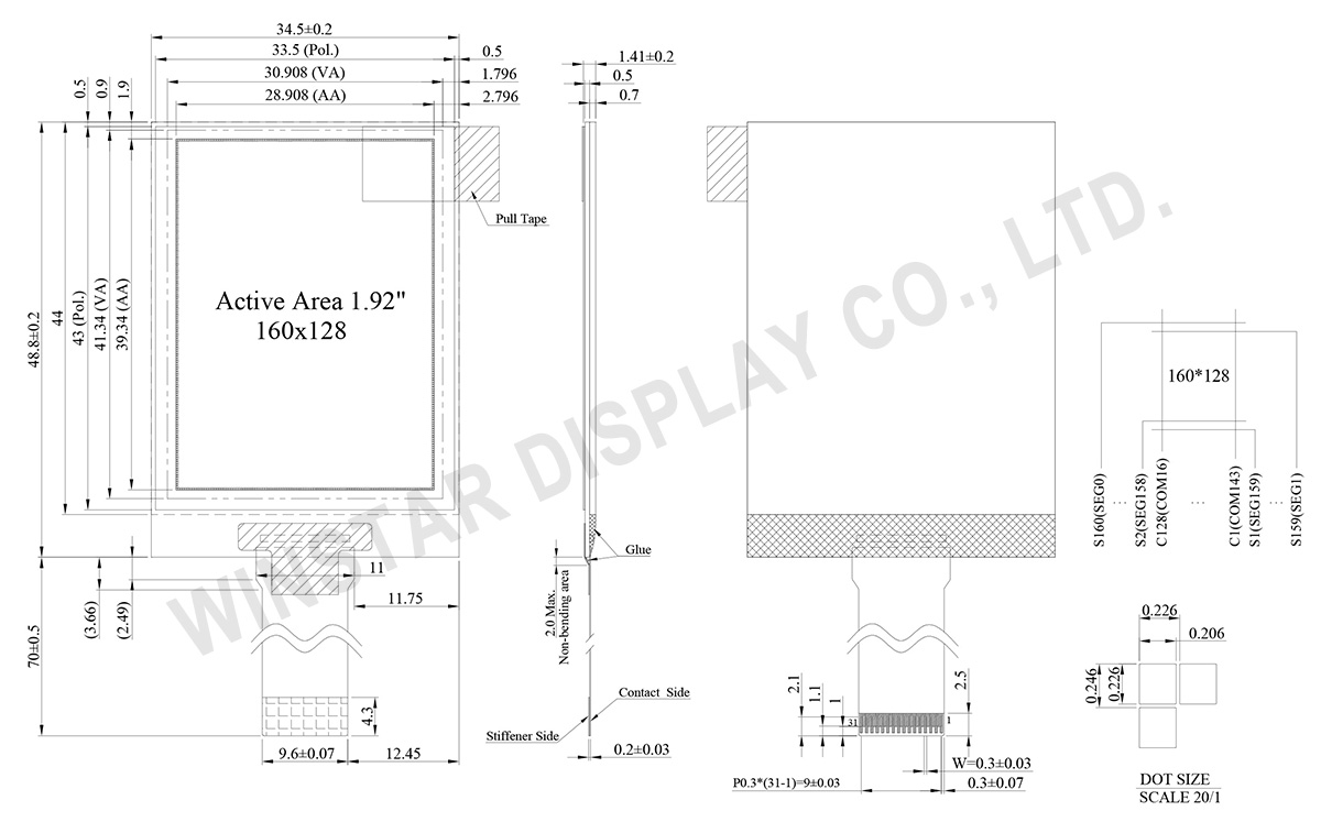
Механические характеристики
| Наименование | Измерения | Единица |
|---|---|---|
| Разрешение | 128 × 160 | точек |
| Габариты | 34.5 × 48.8 × 1.41 | mm |
| Активная область | 28.908 × 39.34 | mm |
| Размер пикселя | 0.206 × 0.226 | mm |
| Шаг пикселя | 0.226 × 0.246 | mm |
| Матрица | Пассивная | |
| Цвет дисплея | монохромные | |
| Рабочий цикл | 1/128 Duty | |
| IC | SH1108 | |
| Интерфейс | 6800, 8080, SPI, I2C | |
| Диагональ | 1.92 дюйма | |
Абсолютные максимальные значения
| Параметр | Символы | Минимальный | Максимальный | Единица |
|---|---|---|---|---|
| Supply Voltage for Logic | VDD | -0.3 | 3.6 | V |
| Supply Voltage for Display | VPP | -0.3 | 17.0 | V |
| Operating Temperature | TOP | -40 | +80 | °C |
| Storage Temperature | TSTG | -40 | +85 | °C |
Электронные характеристики
| Наименование | Символы | Кондиция | Минимальный | Типичный | Максимальный | Единица |
|---|---|---|---|---|---|---|
| Supply Voltage for Logic | VDD | - | 1.65 | 3.0 | 3.5 | V |
| Supply Voltage for Display | VPP | - | 11.5 | 12.0 | 12.5 | V |
| Input High Volt. | VIH | - | 0.8xVDD | - | VDD | V |
| Input Low Volt. | VIL | - | VSS | - | 0.2xVDD | V |
| Output High Volt. | VOH | IOH=-0.5mA | 0.8xVDD | - | VDD | V |
| Output Low Volt. | VOL | IOL=0.5mA | VSS | - | 0.2xVDD | V |
| 50% Check Board Operating Current for VPP | IPP | VPP=12V | - | 23.0 | 35.0 | mA |
