


1.92", 160x128 OLED-Anzeige
Modellnummer WEO160128A
►1,92 Zoll OLED
►Rundes OLED Display
►Typ: Grafik
►Bauweise: COG
►160x128 Punktmatrix
►Integrierter Controller SH1108
►3-V-Stromversorgung
►1/128 duty
►Schnittstelle: 6800, 8080, SPI, I2C
►die Farbe des Displays: Weiß / Gelb
Beschreibung
Das WEO160128A ist ein hochauflösendes 1,92-Zoll Passiv-Matrix-OLED-Display. Dieses Modul verfügt über eine COG-Struktur und hat eine Auflösung von 160x128 Pixeln. Es ist mit dem IC SH1108 ausgestattet und unterstützt die 6800/8080 8-Bit Parallel-, sowie die I2C- und 4-Draht-SPI-Schnittstelle. Es hat eine 3V-Versorgungsspannung für die Logikschaltungen, 12V für das Dispay-Panel und einen 1/64 Tastgrad.
Dieses Modul eignet sich ideal für industrielle Steuergeräte, Smart-Home-Anwendungen, intelligente Technologiegeräte, medizinische Instrumente usw. Das Modul kann bei Temperaturen von -40 ℃ bis 80 ℃ betrieben werden; die Lagertemperatur liegt zwischen -40 °C und 85 °C.
Zeichnung
Data source ref: WEO160128AWPP3N00000
Technische Daten
Schnittstelle Pin-Funktion
| No. | Symbol | Funktion | ||||||||||||||||||||||||
|---|---|---|---|---|---|---|---|---|---|---|---|---|---|---|---|---|---|---|---|---|---|---|---|---|---|---|
| 1 | NC | No connection | ||||||||||||||||||||||||
| 2 | VPP | This is the most positive voltage supply pad of the chip. It should be supplied externally. |
||||||||||||||||||||||||
| 3 | VSEGM | This is a pad for the voltage output level for segment pre-charge. A capacitor should be connected between this pad and VSS. |
||||||||||||||||||||||||
| 4 | VCOMH | This is a pad for the voltage output high level for common signals. A capacitor should be connected between this pad and VSS. |
||||||||||||||||||||||||
| 5 | VSL | This is a segment voltage reference pad. A capacitor should be connected between this pad and VSS. |
||||||||||||||||||||||||
| 6 | NC | No connection | ||||||||||||||||||||||||
| 7 | IREF | This is a segment current reference pad. A resistor should be connected between this pad and VSS. Set the current at 15.625uA. |
||||||||||||||||||||||||
| 8 | VPP | This is the most positive voltage supply pad of the chip. It should be supplied externally. |
||||||||||||||||||||||||
| 9 | NC | No connection | ||||||||||||||||||||||||
| 10 | VSS | Ground for analog, logic & buffer respectively. | ||||||||||||||||||||||||
| 11 | VCL | This is a common voltage reference pad. This pad should be connected to VSS externally. |
||||||||||||||||||||||||
| 12 | VDD | 1.65 - 3.5V power supply input pad for logic. | ||||||||||||||||||||||||
| 13 | IM0 | These are the MPU interface mode select pads.
|
||||||||||||||||||||||||
| 14 | IM1 | |||||||||||||||||||||||||
| 16 | IM2 | |||||||||||||||||||||||||
| 15 | VDD | 1.65 - 3.5Vpower supply input pad | ||||||||||||||||||||||||
| 17 | CS | This pad is the chip select input. When CS = “L”, then the chip select becomes active, and data command I/O is enabled. | ||||||||||||||||||||||||
| 18 | RES | This is a reset signal input pad. When RES is set to “L”, the settings are initialized. The reset operation is performed by the RES signal level. | ||||||||||||||||||||||||
| 19 | A0 | This is the Data/Command control pad that determines whether the data bits are data or a command. A0 = “H”: the inputs at D0 to D7 are treated as display data. A0 = “L”: the inputs at D0 to D7 are transferred to the command registers. In I2C interface, this pad serves as SA0 to distinguish the different address of OLED driver. |
||||||||||||||||||||||||
| 20 | WR | This is a MPU interface input pad. When connected to an 8080 MPU, this is active LOW. This pad connects to the 8080 MPU WR signal. The signals on the data bus are latched at the rising edge of the WR signal. When connected to a 6800 Series MPU: This is the read/write control signal input terminal. When WR = “H”: Read. When WR = “L”: Write. |
||||||||||||||||||||||||
| 21 | RD | This is a MPU interface input pad. When connected to an 8080 series MPU, it is active LOW. This pad is connected to the RD signal of the 8080 series MPU, and the data bus is in an output status when this signal is “L”. When connected to a 6800 series MPU, this is active HIGH. This is used as an enable clock input of the 6800 series MPU. |
||||||||||||||||||||||||
| 22 | D0 | This is an 8-bit bi-directional data bus that connects to an 8-bit or 16-bit standard MPU data bus. When the serial interface is selected, then D0 serves as the serial clock input pad (SCL) and D1 serves as the serial data input pad (SI). At this time, D2 to D7 are set to high impedance. When the I2C interface is selected, then D0 serves as the serial clock input pad (SCL) and D1 serves as the serial data input pad (SDA). At this time, D2 to D7 are set to high impedance. |
||||||||||||||||||||||||
| 23 | D1 | |||||||||||||||||||||||||
| 24 | D2 | |||||||||||||||||||||||||
| 25 | D3 | |||||||||||||||||||||||||
| 26 | D4 | |||||||||||||||||||||||||
| 27 | D5 | |||||||||||||||||||||||||
| 28 | D6 | |||||||||||||||||||||||||
| 29 | D7 | |||||||||||||||||||||||||
| 30 | NC | No connection | ||||||||||||||||||||||||
| 31 | VPP | This is the most positive voltage supply pad of the chip. It should be supplied externally. |
mechanische Daten
| Artikel | Ausmaß | Einheit |
|---|---|---|
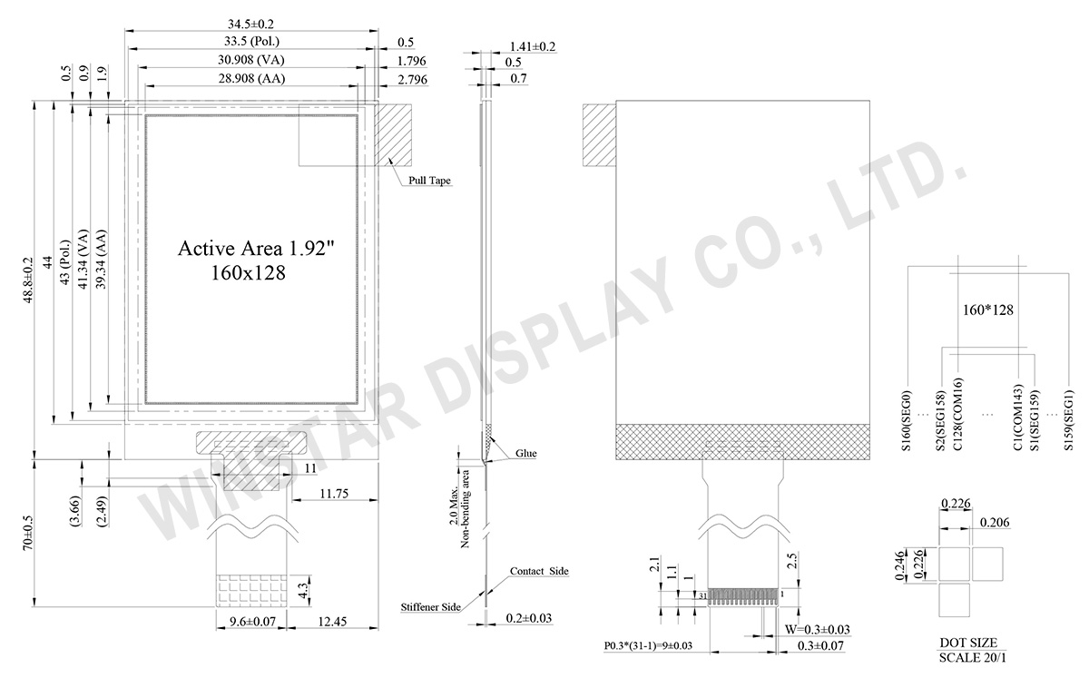
| Punktmatrix | 128 × 160 | Punkte |
| Abmaße der modul | 34,5 × 48,8 × 1,41 | mm |
| Aktiver Bereich | 28,908 × 39,34 | mm |
| Pixelgröße | 0,206 × 0,226 | mm |
| Pixelabstand | 0,226 × 0,246 | mm |
| der Anzeigemodus | Passive Matrix | |
| die Farbe des Displays | Monochrome | |
| Drive Duty | 1/128 Duty | |
| IC | SH1108 | |
| Schnittstelle | 6800, 8080, SPI, I2C | |
| Größe | 1,92 Zoll | |
absolute Grenzwerte
| Parameter | Symbol | Mindestwert | Maximalwert | Einheit |
|---|---|---|---|---|
| Supply Voltage for Logic | VDD | -0,3 | 3,6 | V |
| Supply Voltage for Display | VPP | -0,3 | 17,0 | V |
| Betriebstemperatur | TOP | -40 | +80 | °C |
| Lagertemperatur | TSTG | -40 | +85 | °C |
elektronische Eingenschaften
| Artikel | Symbol | Bedingung | Mindestwert | typischer Wert | Maximalwert | Einheit |
|---|---|---|---|---|---|---|
| Supply Voltage for Logic | VDD | - | 1,65 | 3,0 | 3,5 | V |
| Supply Voltage for Display | VPP | - | 11,5 | 12,0 | 12,5 | V |
| Input High Volt. | VIH | - | 0,8xVDD | - | VDD | V |
| Input Low Volt. | VIL | - | VSS | - | 0,2xVDD | V |
| Output High Volt. | VOH | IOH=-0,5mA | 0,8xVDD | - | VDD | V |
| Output Low Volt. | VOL | IOL=0,5mA | VSS | - | 0,2xVDD | V |
| 50% Check Board Operating Current for VPP | IPP | VPP=12V | - | 23,0 | 35,0 | mA |

")


