


製品情報
WEO160128Aは1.92インチの高解像度パッシブマトリクスOLEDディスプレイモジュールで、160x128ドットの解像度で作られたCOG構造にします。このモジュールにはSH1108 ICが内蔵されて、6800/8080・8ビットパラレルにして、I2C及び4-Wire SPIインタフェースを使用できて、ロジック3V用電源電圧で、ディスプレイ12V用電源電圧で、1/128デューティサイクルにします。
このモジュールは産業用制御機器、スマートホームアプリケーション、インテリジェントテクノロジー機器、医療機器等に最適です。 -40℃〜 80℃で動作可能で、 保存温度範囲は-40℃〜 85℃です。
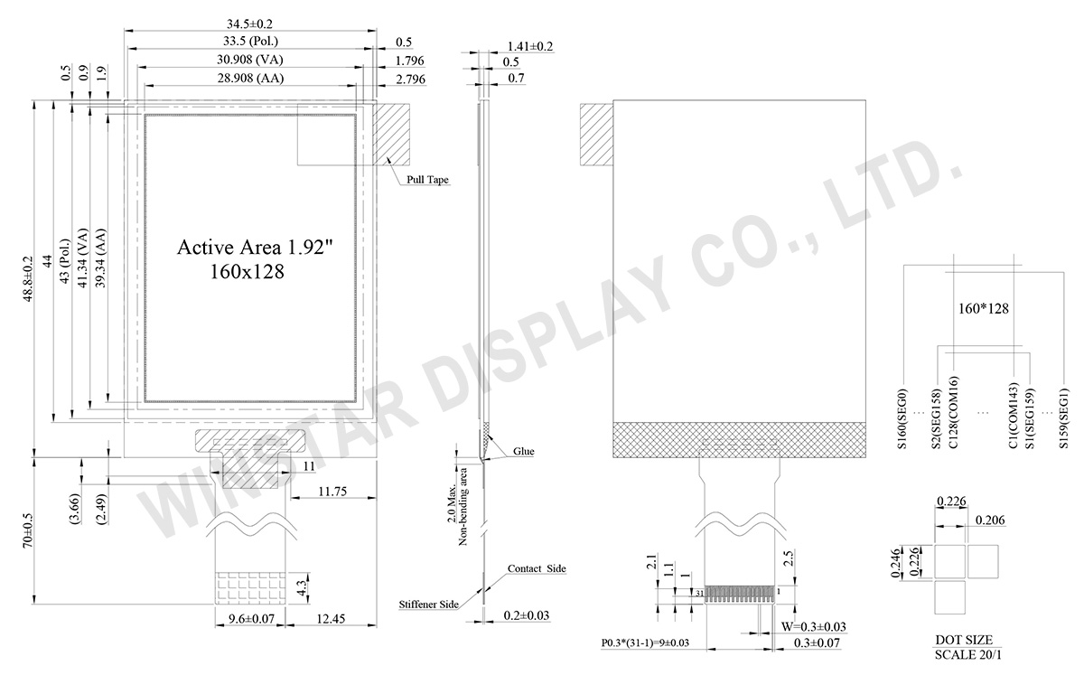
外形図
Data source ref: WEO160128AWPP3N00000
製品仕様
ピン功能定義
| No. | 記号 | 説明 | ||||||||||||||||||||||||
|---|---|---|---|---|---|---|---|---|---|---|---|---|---|---|---|---|---|---|---|---|---|---|---|---|---|---|
| 1 | NC | No connection | ||||||||||||||||||||||||
| 2 | VPP | This is the most positive voltage supply pad of the chip. It should be supplied externally. |
||||||||||||||||||||||||
| 3 | VSEGM | This is a pad for the voltage output level for segment pre-charge. A capacitor should be connected between this pad and VSS. |
||||||||||||||||||||||||
| 4 | VCOMH | This is a pad for the voltage output high level for common signals. A capacitor should be connected between this pad and VSS. |
||||||||||||||||||||||||
| 5 | VSL | This is a segment voltage reference pad. A capacitor should be connected between this pad and VSS. |
||||||||||||||||||||||||
| 6 | NC | No connection | ||||||||||||||||||||||||
| 7 | IREF | This is a segment current reference pad. A resistor should be connected between this pad and VSS. Set the current at 15.625uA. |
||||||||||||||||||||||||
| 8 | VPP | This is the most positive voltage supply pad of the chip. It should be supplied externally. |
||||||||||||||||||||||||
| 9 | NC | No connection | ||||||||||||||||||||||||
| 10 | VSS | Ground for analog, logic & buffer respectively. | ||||||||||||||||||||||||
| 11 | VCL | This is a common voltage reference pad. This pad should be connected to VSS externally. |
||||||||||||||||||||||||
| 12 | VDD | 1.65 - 3.5V power supply input pad for logic. | ||||||||||||||||||||||||
| 13 | IM0 | These are the MPU interface mode select pads.
|
||||||||||||||||||||||||
| 14 | IM1 | |||||||||||||||||||||||||
| 16 | IM2 | |||||||||||||||||||||||||
| 15 | VDD | 1.65 - 3.5Vpower supply input pad | ||||||||||||||||||||||||
| 17 | CS | This pad is the chip select input. When CS = “L”, then the chip select becomes active, and data command I/O is enabled. | ||||||||||||||||||||||||
| 18 | RES | This is a reset signal input pad. When RES is set to “L”, the settings are initialized. The reset operation is performed by the RES signal level. | ||||||||||||||||||||||||
| 19 | A0 | This is the Data/Command control pad that determines whether the data bits are data or a command. A0 = “H”: the inputs at D0 to D7 are treated as display data. A0 = “L”: the inputs at D0 to D7 are transferred to the command registers. In I2C interface, this pad serves as SA0 to distinguish the different address of OLED driver. |
||||||||||||||||||||||||
| 20 | WR | This is a MPU interface input pad. When connected to an 8080 MPU, this is active LOW. This pad connects to the 8080 MPU WR signal. The signals on the data bus are latched at the rising edge of the WR signal. When connected to a 6800 Series MPU: This is the read/write control signal input terminal. When WR = “H”: Read. When WR = “L”: Write. |
||||||||||||||||||||||||
| 21 | RD | This is a MPU interface input pad. When connected to an 8080 series MPU, it is active LOW. This pad is connected to the RD signal of the 8080 series MPU, and the data bus is in an output status when this signal is “L”. When connected to a 6800 series MPU, this is active HIGH. This is used as an enable clock input of the 6800 series MPU. |
||||||||||||||||||||||||
| 22 | D0 | This is an 8-bit bi-directional data bus that connects to an 8-bit or 16-bit standard MPU data bus. When the serial interface is selected, then D0 serves as the serial clock input pad (SCL) and D1 serves as the serial data input pad (SI). At this time, D2 to D7 are set to high impedance. When the I2C interface is selected, then D0 serves as the serial clock input pad (SCL) and D1 serves as the serial data input pad (SDA). At this time, D2 to D7 are set to high impedance. |
||||||||||||||||||||||||
| 23 | D1 | |||||||||||||||||||||||||
| 24 | D2 | |||||||||||||||||||||||||
| 25 | D3 | |||||||||||||||||||||||||
| 26 | D4 | |||||||||||||||||||||||||
| 27 | D5 | |||||||||||||||||||||||||
| 28 | D6 | |||||||||||||||||||||||||
| 29 | D7 | |||||||||||||||||||||||||
| 30 | NC | No connection | ||||||||||||||||||||||||
| 31 | VPP | This is the most positive voltage supply pad of the chip. It should be supplied externally. |
規格説明
| 項目 | 仕様 | 単位 |
|---|---|---|
| ドットマトリックス(解像度) | 128 × 160 | Dots |
| 外形寸法 | 34.5 × 48.8 × 1.41 | mm |
| 有効表示エリア | 28.908 × 39.34 | mm |
| ドットサイズ | 0.206 × 0.226 | mm |
| ドットピッチ | 0.226 × 0.246 | mm |
| 表示モード | パッシブマトリクス | |
| 発光色 | モノクロ | |
| 駆動方法 | 1/128 Duty | |
| IC | SH1108 | |
| インターフェイス | 6800, 8080, SPI, I2C | |
| サイズ | 1.92 インチ | |
絶対最大定格
| パラメーター | 記号 | 最小値 | 最大値 | 単位 |
|---|---|---|---|---|
| ロジック電源電圧 | VDD | -0.3 | 3.6 | V |
| Display電源電圧 | VPP | -0.3 | 17.0 | V |
| 操作温度 | TOP | -40 | +80 | °C |
| 保存温度 | TSTG | -40 | +85 | °C |
電気特性
| 項目 | 記号 | 条件 | 最小値 | 典型値 | 最大値 | 単位 |
|---|---|---|---|---|---|---|
| ロジック電源電圧 | VDD | - | 1.65 | 3.0 | 3.5 | V |
| Display電源電圧 | VPP | - | 11.5 | 12.0 | 12.5 | V |
| 入力電圧(High) | VIH | - | 0.8xVDD | - | VDD | V |
| 入力電圧(Low) | VIL | - | VSS | - | 0.2xVDD | V |
| 出力電圧(High) | VOH | IOH=-0.5mA | 0.8xVDD | - | VDD | V |
| 出力電圧(Low) | VOL | IOL=0.5mA | VSS | - | 0.2xVDD | V |
| 50% Check Board Operating Current for VPP | IPP | VPP=12V | - | 23.0 | 35.0 | mA |
