


产品叙述
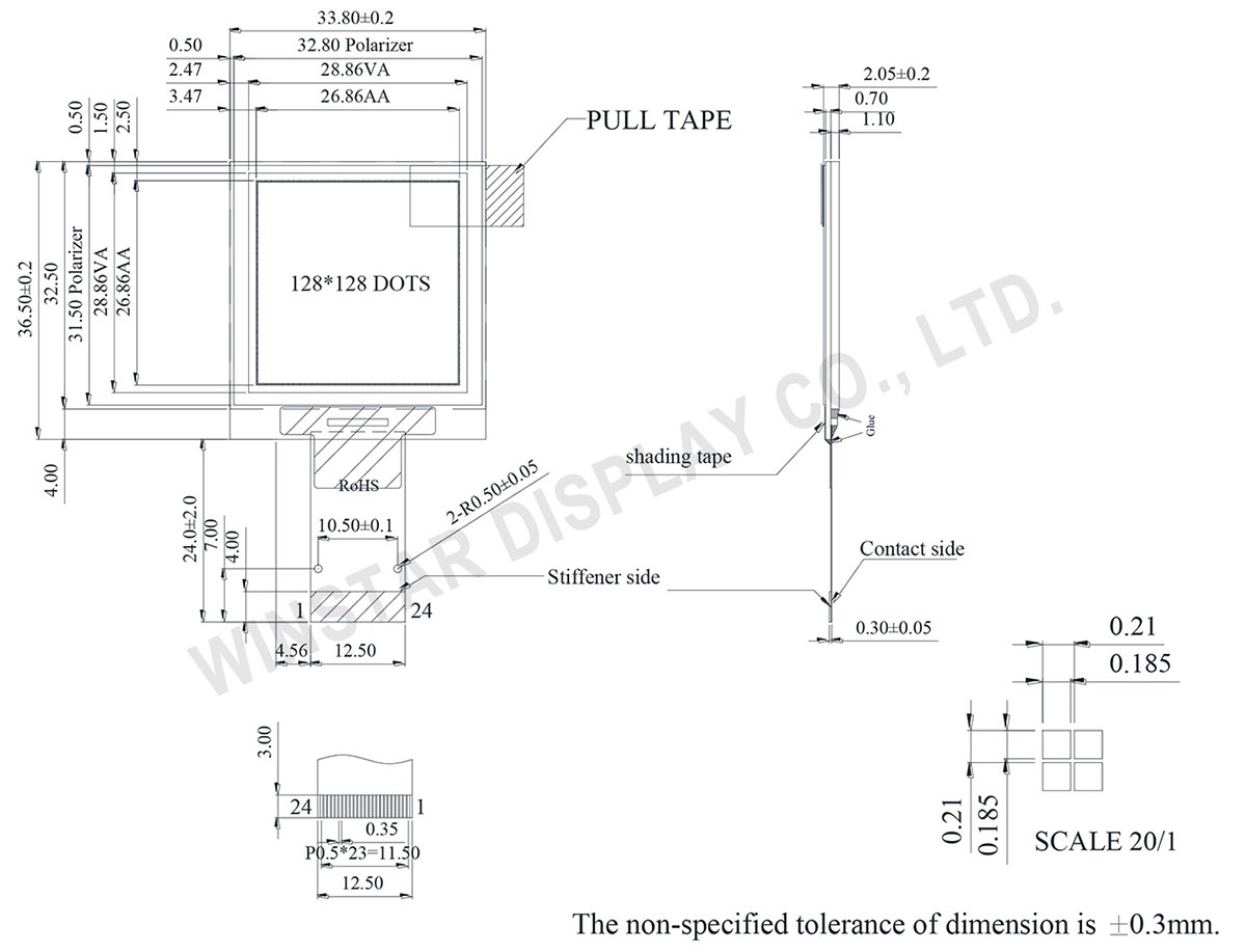
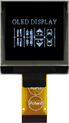
WEO128128A 是一款1.5吋单色被动式OLED显示器模块,分辨率为128x128 pixels。WEO128128A内建SSD1327 controller控制器, 支持多种传输接口: 6800 8-bite, 8080 8-bit 并行接口, I2C 与4线SPI串行接口。WEO128128A的模块尺寸为33.8 x 36.5 mm,AA区尺寸26.86 x 26.83 mm, 3V驱动。WEO128128A为COG结构的OLED显示器模块,为有机自发光,无须背光源,因此模块轻薄且低耗电流,此款WEO128128A模块非常适合手持式产品、量测仪器、物联网装置、工控设备等等。
此模块的工作温度是-40℃至+80℃,储存温度-40℃至+80℃,如有产品需求或是需要更详细信息请与我们联系。
规格图
产品规格
Pin功能定义
| No. | 符号 | 功能说明 | ||||||||||
|---|---|---|---|---|---|---|---|---|---|---|---|---|
| 1 | VSS | Ground pin. It must be connected to external ground. | ||||||||||
| 2 | VCC | Power supply for panel driving voltage. This is also the most positive power voltage supply pin. It is supplied by external high voltage source. | ||||||||||
| 3 | VCOMH | COM signal deselected voltage level. A capacitor should be connected between this pin and VSS. No external power supply is allowed to connect to this pin. |
||||||||||
| 4 | VCI | Low voltage power supply and power supply for interface logic level. It should match with the MCU interface voltage level and must be connected to external source. VCI must always set to be equivalent to or higher than VDD. |
||||||||||
| 5 | VDD | Power supply pin for core logic operation. | ||||||||||
| 6 | BS1 | MCU bus interface selection pins. Select appropriate logic setting as described in the following table. BS2 and BS1 are pin select. Bus Interface selection
Note (1) 0 is connected to VSS (2) 1 is connected to VCI |
||||||||||
| 7 | BS2 | |||||||||||
| 8 | VSS | Ground pin. It must be connected to external ground. | ||||||||||
| 9 | IREF | This pin is the segment output current reference pin | ||||||||||
| 10 | CS# | This pin is the chip select input connecting to the MCU. The chip is enabled for MCU communication only when CS# is pulled LOW (active LOW). |
||||||||||
| 11 | RES# | This pin is reset signal input. When the pin is pulled LOW, initialization of the chip is executed. Keep this pin pull HIGH during normal operation. |
||||||||||
| 12 | D/C | This pin is Data/Command control pin connecting to the MCU. When the pin is pulled HIGH, the data at D[7:0] will be interpreted as data. When the pin is pulled LOW, the data at D[7:0] will be transferred to a command register. In I2C mode, this pin acts as SA0 for slave address selection. When 3-wire serial interface is selected, this pin must be connected to VSS. |
||||||||||
| 13 | W/R# | This pin is read / write control input pin connecting to the MCU interface. When 6800 interface mode is selected, this pin will be used as Read/Write (R/W#) selection input. Read mode will be carried out when this pin is pulled HIGH and write mode when LOW. When 8080 interface mode is selected, this pin will be the Write (WR#) input. Data write operation is initiated when this pin is pulled LOW and the chip is selected. |
||||||||||
| 14 | RD# | This pin is MCU interface input. When 6800 interface mode is selected, this pin will be used as the Enable (E) signal. Read/write operation is initiated when this pin is pulled HIGH and the chip is selected. When 8080 interface mode is selected, this pin receives the Read (RD#) signal. Read operation is initiated when this pin is pulled LOW and the chip is selected. When serial or I2C interface is selected, this pin must be connected to VSS. |
||||||||||
| 15 | D0 | These pins are bi-directional data bus connecting to the MCU data bus. Unused pins are recommended to tie LOW. When serial interface mode is selected, D0 will be the serial clock input: SCLK; D1 will be the serial data input: SDIN and D2 should be kept NC. When I2C mode is selected, D2, D1 should be tied together and serve as SDAout, SDAin in application and D0 is the serial clock input, SCL. |
||||||||||
| 16 | D1 | |||||||||||
| 17 | D2 | |||||||||||
| 18 | D3 | |||||||||||
| 19 | D4 | |||||||||||
| 20 | D5 | |||||||||||
| 21 | D6 | |||||||||||
| 22 | D7 | |||||||||||
| 23 | VCC | Power supply for panel driving voltage. This is also the most positive power voltage supply pin. It is supplied by external high voltage source. | ||||||||||
| 24 | VSS | Ground pin. |
规格说明
| 项目 | 尺寸 | 单位 |
|---|---|---|
| 点阵 | 128 x 128 Dots | - |
| 模块尺寸 | 33.80 x 36.50 x 2.05 | mm |
| 有效区域 | 26.86 x 26.86 | mm |
| 像素大小 | 0.185 x 0.185 | mm |
| 像素间距 | 0.210 x 0.210 | mm |
| 显示模式 | 被动矩阵 | |
| 发光颜色 | 单色 | |
| 驱动方式 | 1/128Duty | |
| IC | SSD1327 | |
| 接口 | 6800,8080,SPI,I2C | |
| 尺寸 | 1.5 寸 | |
最大绝对额定
| 参数 | 符号 | 最小值 | 最大值 | 单位 |
|---|---|---|---|---|
| 工作电源电压 | VCI | -0.3 | 4.0 | V |
| 逻辑电源电压 | VDD | -0.5 | 2.75 | V |
| 显示电源电压 | VCC | -0.5 | 19.0 | V |
| 工作温度 | TOP | -40 | +80 | °C |
| 储存温度 | TSTG | -40 | +85 | °C |
电气特性
| 项目 | 符号 | 条件 | 最小值 | 典型值 | 最大值 | 单位 |
|---|---|---|---|---|---|---|
| 逻辑电源电压 | VCI | Note | 2.8 | 3.0 | 3.3 | V |
| 显示电源电压 | VCC | - | 14 | 14.5 | 15 | V |
| 输入高准位 | VIH | - | 0.8×VCI | - | VCI | V |
| 输入低准位 | VIL | - | 0 | - | 0.2×VCI | V |
| 输出高准位 | VOH | - | 0.9×VCI | - | VCI | V |
| 输出低准位 | VOL | - | 0 | - | 0.1×VCI | V |
| 50% Check Board operating Current | VCC =14.5V | - | 24 | 30 | mA | |
FPC options
| Drawing | FPC Length | PIN | Pitch | ZIF FPC or HOTBAR FPC | Interface | FPC No. | Create Date |
|---|---|---|---|---|---|---|---|
 |
25.05 | 24 | 0.5 | ZIF | 6800,8080,SPI,I2C | FPC2050002411XXXXX03 | 20150901 |
 |
41 | 24 | 0.5 | ZIF | 6800,8080,4-Wire SPI,I2C | FPC2050002411XXXXX12 | 20200116 |
Search keyword: 128x128 oled, oled 128x128, 1.5 oled, 1.5" oled, 1.5寸 oled, oled 1.5寸, oled 1.5"


 - WF50BTIFGDHTV")


