


製品情報
WO240128Bは単色のCOG LCDモジュールです。240x128ドットの解像度で4.8インチのグラフィック製品です。ST7586S IC内臓で、6800 8-bit、8080 8-bit パラレスと3-線式9-bit /4-線式8-bitのSPIインターフェースを支援しています。COG構造ですが、表示エリア(VA)サイズと有効表示エリア(AA)サイズはウィンスター社COB標準品のWG240128Bと同様です。WO240128BはCOG構造ですので、より薄くて消費電流と給電電圧が低くなる特性はあります。4.8インチモジュールを採用する新規開発案にお薦めです。
WO240128Bは動作温度が-20℃~+70℃で、保存温度が-30℃~+80℃です。STN ネガティブと FSTN ポジティブのパネルは選択できて、白発光のLEDバックライトを搭載しています。そして、WO240128Bの仕様概要は以下の通りで、何卒ご参照ください。
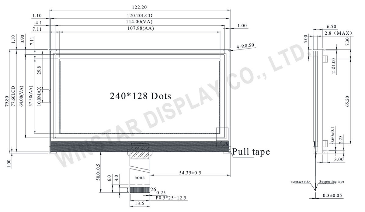
外形図
製品仕様
ピン功能定義
| Pin No. | 記号 | 説明 |
|---|---|---|
| 1 | ESD GND | Electro-Static discharge |
| 2 | VG | VG is the power of SEG-drivers |
| 3 | XV0 | Negative operating voltage of COM-drivers |
| 4 | V0 | Positive operating voltage of COM-drivers |
| 5 | VM | VM is the non-select voltage level of COM-drivers |
| 6 | VDDA | Power supply |
| 7 | VSS | Ground |
| 8 | VD1 | Digital power source selection |
| 9 | VDDI | VDD1 is the power of interface I/O circuit |
| 10 | CSB | Chip select input pin CSB=“L”: This chip is selected and the MPU interface is active CSB=“H”: This chip is not selected and the MPU interface is disabled (D[7:0] are high impedance) |
| 11 12 13 |
IF3 IF2 IF1 |
These pins select interface operation mode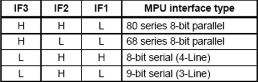 Note: Refer to “Interface Selection” for detailed information |
| 14 | RSTB | Reset input pin. When RSTB is “L”, internal initialization procedure is executed |
| 15 | /RD(E) | Read / Write execution control pin. (This pin is only used in parallelinterface)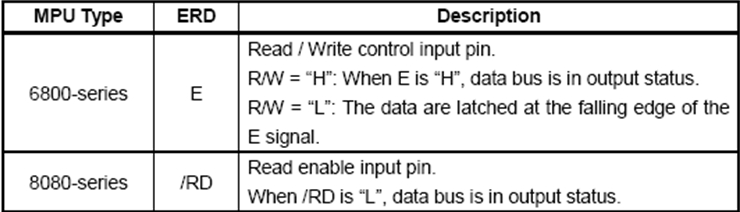 This pin is not used in serial interfaces and should be connected to VDD1 |
| 16~23 | D7~D0 | The bi-directional data bus of the MPU interface. When CSB is “H”, they are high impedance If using serial interface: D0 is the SDA signal in 4-Line & 3-Line interface D1 is the A0 signal in 4-Line interface |
| 24 | /WR/(R/W) | Read / Write execution control pin. (This pin is only used in parallel interface)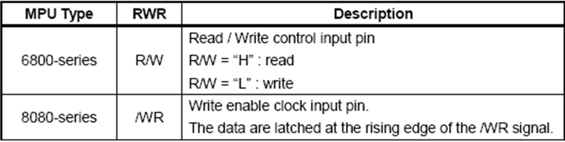 This pin is not used in serial interfaces and should be connected to VDD1 |
| 25 | A0(SCL) | The function of this pin is different in parallel and serial interface In parallel interface: A0 is register selection input A0 = "H": inputs on data bus are display data A0 = "L": inputs on data bus are command In serial interface: this pad will be used as SCL (serial-clock) input |
| 26 | ESD GND | Electro-Static discharge |
規格説明
| 項目 | 標準値 | 単位 |
|---|---|---|
| ドットマトリクス(解像度) | 240 x 128 | - |
| モジュールサイズ | 122.2 x 79.8 x 6.5 | mm |
| 表示エリア | 114.0 x 64.0 | mm |
| 有効エリア | 107.98 x 57.58 | mm |
| ドットサイズ | 0.43 x 0.43 | mm |
| ドットピッチ | 0.45 x 0.45 | mm |
| 駆動方式 | 1/128Duty,1/12Bias | |
| バックライトタイプ | LED | |
| IC | ST7586S | |
絶対最大定格
| 項目 | 記号 | 最小値 | 標準値 | 最大値 | 単位 |
|---|---|---|---|---|---|
| 動作温度 | TOP | -20 | - | +70 | ℃ |
| 保存温度 | TST | -30 | - | +80 | ℃ |
| Digital電源電圧 | VDDI | -0.3 | - | 3.6 | V |
| Analog電源電圧 | VDDA | -0.3 | - | 3.6 | V |
| LCD電源電圧 | V0-XV0 | -0.3 | - | 19 | V |
| LCD電源電圧 | VG | -0.3 | - | 5.5 | V |
電気特性
| 項目 | 記号 | 条件 | 最小値 | 標準値 | 最大値 | 単位 |
|---|---|---|---|---|---|---|
| ロジック電源電圧 | VDD-VSS | - | 3.0 | 3.3 | 3.6 | V |
| LCM電源電圧 | VOP | Ta=-20℃ Ta=25℃ Ta=+70℃ |
- 14.8 - |
- 15.0 - |
- 15.2 - |
V V V |
| 入力電圧(High) | VIH | - | 0.7VDD | - | VDD | V |
| 入力電(流Low) | VIL | - | Vss | - | 0.3 VDD | V |
| 出力電圧(High) | VOH | - | 0.8 VDD | - | VDD | V |
| 出力電圧(Low) | VOL | - | Vss | - | 0.2VDD | V |
| 電源電流 | IDD | VDD=3.3V | - | - | 2.0 | mA |
Search keyword: 240x128 lcd, 240 x 128 lcd, lcd 240x128, lcd 240 x 128


