


產品敘述
WO240128B單色COG LCD液晶顯示器是一款240x128點陣式4.8吋的繪圖型模組。WO240128B內建ST7586S 控制器IC, 支援多種傳輸介面: 6800 8-bit, 8080 8-bit 平行介面與3-線9-bit /4-線8-bit 串列SPI介面。WO240128B為COG結構模組,其VA區尺寸以及AA區尺寸與現有華凌標準品COB結構的WG240128B相同,但WO240128B為COG結構,所以模組厚度較薄,外形輕巧,具有低功耗,低供電等特點,客戶若有需求4.8吋模組的新案開發,建議可採用此WO240128B模組。
WO240128B的工作溫度是-20℃至+70℃,儲存溫度-30℃至+80℃,此型號目前有STN Negative 負顯, 與 FSTN positive正顯兩種玻璃可供選擇,可搭配LED白光,如有需求其他LCD或是LED背光組合可與我們聯繫。
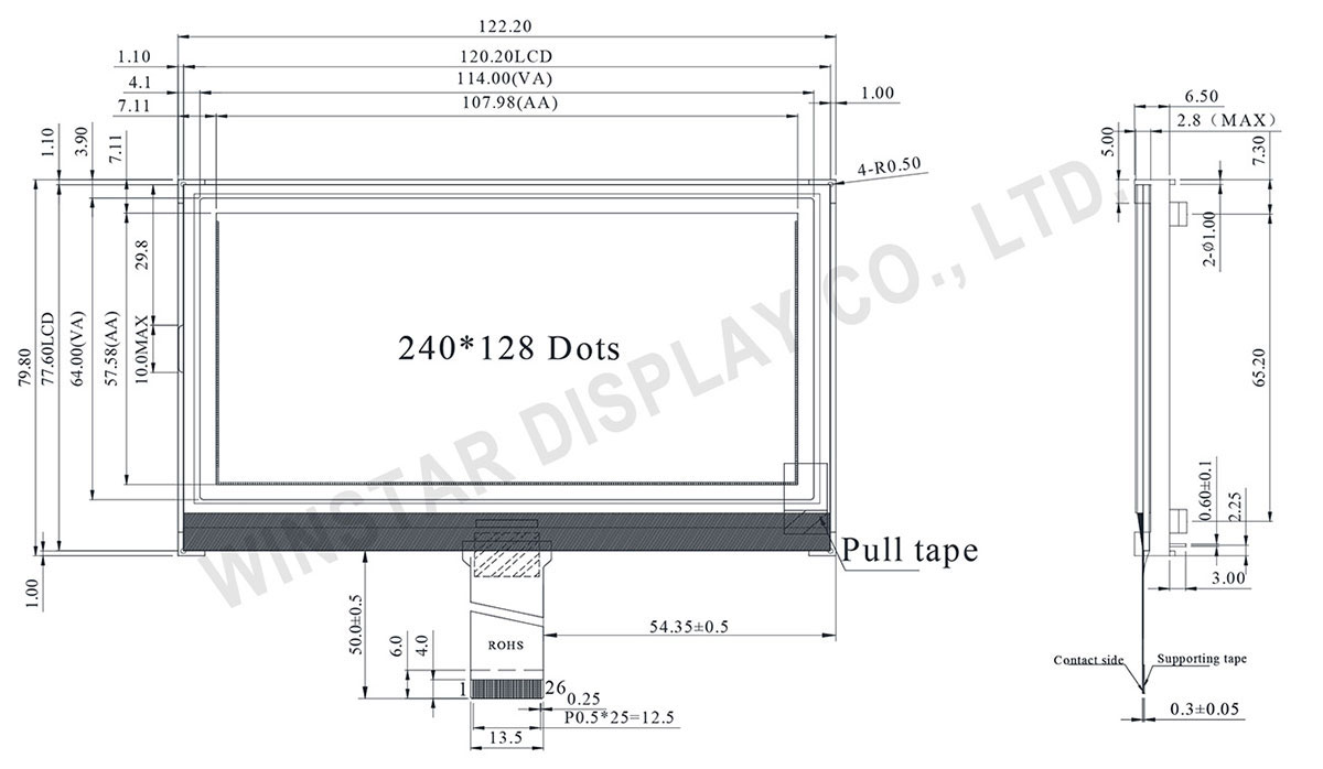
規格圖
產品規格
Pin功能定義
| Pin No. | 符號 | 說明 |
|---|---|---|
| 1 | ESD GND | Electro-Static discharge |
| 2 | VG | VG is the power of SEG-drivers |
| 3 | XV0 | Negative operating voltage of COM-drivers |
| 4 | V0 | Positive operating voltage of COM-drivers |
| 5 | VM | VM is the non-select voltage level of COM-drivers |
| 6 | VDDA | Power supply |
| 7 | VSS | Ground |
| 8 | VD1 | Digital power source selection |
| 9 | VDDI | VDD1 is the power of interface I/O circuit |
| 10 | CSB | Chip select input pin CSB=“L”: This chip is selected and the MPU interface is active CSB=“H”: This chip is not selected and the MPU interface is disabled (D[7:0] are high impedance) |
| 11 12 13 |
IF3 IF2 IF1 |
These pins select interface operation mode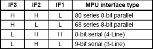 Note: Refer to “Interface Selection” for detailed information |
| 14 | RSTB | Reset input pin. When RSTB is “L”, internal initialization procedure is executed |
| 15 | /RD(E) | Read / Write execution control pin. (This pin is only used in parallelinterface)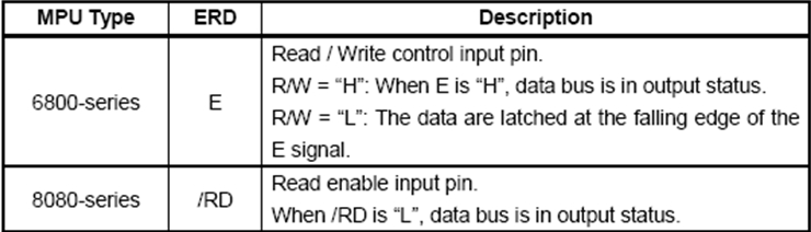 This pin is not used in serial interfaces and should be connected to VDD1 |
| 16~23 | D7~D0 | The bi-directional data bus of the MPU interface. When CSB is “H”, they are high impedance If using serial interface: D0 is the SDA signal in 4-Line & 3-Line interface D1 is the A0 signal in 4-Line interface |
| 24 | /WR/(R/W) | Read / Write execution control pin. (This pin is only used in parallel interface)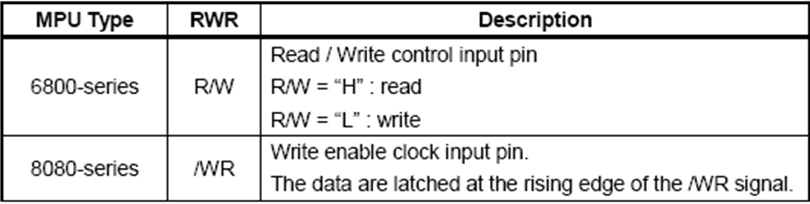 This pin is not used in serial interfaces and should be connected to VDD1 |
| 25 | A0(SCL) | The function of this pin is different in parallel and serial interface In parallel interface: A0 is register selection input A0 = "H": inputs on data bus are display data A0 = "L": inputs on data bus are command In serial interface: this pad will be used as SCL (serial-clock) input |
| 26 | ESD GND | Electro-Static discharge |
規格說明
| 項目 | 標準尺寸 | 單位 |
|---|---|---|
| 點陣(解析度) | 240 x 128 | - |
| 模組尺寸 | 122.2 x 79.8 x 6.5 | mm |
| 檢視區域 | 114.0 x 64.0 | mm |
| 有效區域 | 107.98 x 57.58 | mm |
| 點大小 | 0.43 x 0.43 | mm |
| 點間距 | 0.45 x 0.45 | mm |
| 驅動方式 | 1/128Duty,1/12Bias | |
| 背光類型 | LED | |
| IC | ST7586S | |
最大絕對額定值
| 項目 | 符號 | 最小值 | 標準值 | 最大值 | 單位 |
|---|---|---|---|---|---|
| 工作溫度 | TOP | -20 | - | +70 | ℃ |
| 儲存溫度 | TST | -30 | - | +80 | ℃ |
| LCD數位電源電壓 | VDDI | -0.3 | - | 3.6 | V |
| 類比電源電壓 | VDDA | -0.3 | - | 3.6 | V |
| LCD電源電壓 | V0-XV0 | -0.3 | - | 19 | V |
| LCD電源電壓 | VG | -0.3 | - | 5.5 | V |
電氣特性
| 項目 | 符號 | 條件 | 最小值 | 標準值 | 最大值 | 單位 |
|---|---|---|---|---|---|---|
| 邏輯電源電壓 | VDD-VSS | - | 3.0 | 3.3 | 3.6 | V |
| LCM電源電壓 | VOP | Ta=-20℃ Ta=25℃ Ta=+70℃ |
- 14.8 - |
- 15.0 - |
- 15.2 - |
V V V |
| 輸入高電壓 | VIH | - | 0.7VDD | - | VDD | V |
| 輸入低電壓 | VIL | - | Vss | - | 0.3 VDD | V |
| 輸出高電壓 | VOH | - | 0.8 VDD | - | VDD | V |
| 輸出低電壓 | VOL | - | Vss | - | 0.2VDD | V |
| 電源電流 | IDD | VDD=3.3V | - | - | 2.0 | mA |
Search keyword: 240x128 lcd, 240 x 128 lcd, lcd 240x128, lcd 240 x 128
