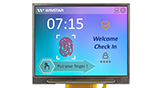
Model No. WEO012864J-CTP
►Tipo: Gráfico
►Estrutura: COG+PCB
►Tamanho: 2,42 polegadas
►Matriz de pontos 128x64
►Controlador SSD1309 integrado
►Alimentação 3V
►1/64 duty
►Interface: 8080 opção 6800, SPI, I2C
►Com painel de toque capacitivo (CTP)
►Detect Point : 1 Finger
►Display Color: Branco / Amarelo / Céu azul / Verde
DRAWING
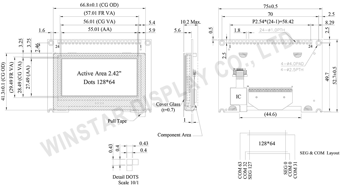
Data source ref: WEO012864JWPP3D00000
SPECIFICATIONS
Interface Pin Function
| No. | Symbol | Function |
|---|---|---|
| 1 | VDD | Power supply pin for core logic operation |
| 2 | VSS | Ground. |
| 3 | NC(GND) | No connection |
| 4~11 | D0~D7 | These pins are bi-directional data bus connecting to the MCU data bus. Unused pins are recommended to tie LOW. |
| 12 | CS# | This pin is the chip select input connecting to the MCU. The chip is enabled for MCU communication only when CS# is pulled LOW (active LOW). |
| 13 | NC(GND) | No connection |
| 14 | RES# | This pin is reset signal input. When the pin is pulled LOW, initialization of the chip is executed. Keep this pin pull HIGH during normal operation. |
| 15 | R/W# | This pin is read / write control input pin connecting to the MCU interface. When 6800 interface mode is selected, this pin will be used as Read/Write (R/W#) selection input. Read mode will be carried out when this pin is pulled HIGH and write mode when LOW. |
| 16 | D/C# | This pin is Data/Command control pin connecting to the MCU. When the pin is pulled HIGH, the data at D[7:0] will be interpreted as data. When the pin is pulled LOW, the data at D[7:0] will be transferred to a command register. |
| 17 | E | This pin is MCU interface input. When 6800 interface mode is selected, this pin will be used as the Enable (E) signal. |
| 18 | NC(GND) | No connection |
| 19 | DISP | No Connection |
| 20 | NC(GND) | No connection |
| 21 | TP_INT | Interrupt signal, active low, asserted to request Host start a new transaction |
| 22 | TP_SDA | I2C data signal |
| 23 | TP_SCL | I2C clock signal |
| 24 | TP_RST | External reset signal, active low |
Mechanical Data
| Item | Dimension | Unit |
|---|---|---|
| Dot Matrix | 128 x 64 | - |
| Module dimension | 75.0 × 52.7 ×10.2 MAX | mm |
| Active Area | 55.01 × 27.49 | mm |
| Pixel Size | 0.40 × 0.40 | mm |
| Pixel Pitch | 0.43 × 0.43 | mm |
| Display Mode | Passive Matrix | |
| Display Color | Monochrome | |
| Drive Duty | 1/64 Duty | |
| IC | SSD1309 | |
| Interface | 8Bits 6800 , Optional 8080 / 4-SPI / I2C | |
| Size | 2.42 inch | |
| PCAP IC | GT911 | |
| Detect Point | 1 | |
| PCAP Interface | I2C | |
| Surface | Normal Glare | |
Absolute Maximum Ratings
| Parameter | Symbol | Min | Max | Unit |
|---|---|---|---|---|
| Supply Voltage for Logic | VDD | -0.3 | 4 | V |
| Operating Temperature | TOP | -20 | +70 | °C |
| Storage Temperature | TSTG | -30 | +80 | °C |
Electronical Characteristics
DC Electrical Characteristics
| Item | Symbol | Condition | Min | Typ | Max | Unit |
|---|---|---|---|---|---|---|
| Supply Voltage for Logic | VDD | - | 2.8 | 3.0 | 3.3 | V |
| High Level Input | VIH | - | 0.8×VDD | - | - | V |
| Low Level Input | VIL | - | - | - | 0.2×VDD | V |
| High Level Output | VOH | - | 0.9×VDD | - | - | V |
| Low Level Output | VOL | - | - | - | 0.1×VDD | V |
| 50% Check Board operating Current | IDD | VDD =3V | - | 150 | 300 | mA |