


产品叙述
WEO128128D-CTP是一款圆形直径1.18寸绘图形OLED显示器,分辨率为128x128 dots搭配电容触控面板。此模块内置SSD1327 IC,支持4线SPI和I2C接口,逻辑电压为3V (typical),驱动方式1/128 duty。WEO128128D-CTP模块内建IT7259触控面板IC使用I2C接口,电容式触控面板支持1指触控。
这款搭配CTP触控面板的圆形OLED非常适合用于智能家居 / 家电应用、能源系统、通信系统、医疗仪器等。模块可在-20℃至+50℃温度下工作; 储存温度为-30℃至+70℃。
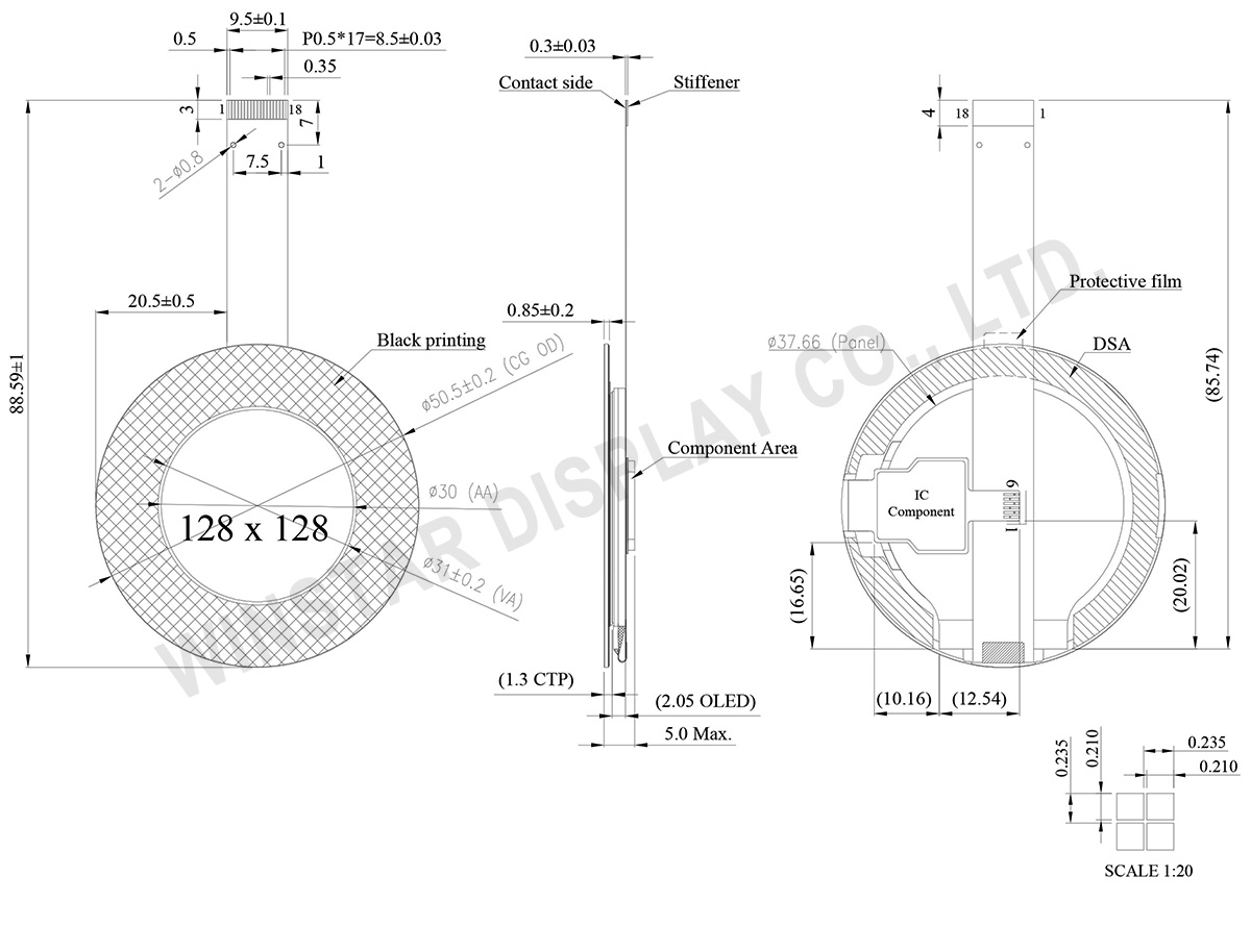
规格图
产品规格
Pin功能定义
| No. | 符号 | 功能说明 | ||||||
|---|---|---|---|---|---|---|---|---|
| 1 | VSS | Ground pin. It must be connected to external ground. | ||||||
| 2 | VCC | Power supply for panel driving voltage. This is also the most positive power voltage supply pin. It is supplied by external high voltage source. | ||||||
| 3 | VCOMH | COM signal deselected voltage level. A capacitor should be connected between this pin and VSS. No external power supply is allowed to connect to this pin. |
||||||
| 4 | VCI | Low voltage power supply and power supply for interface logic level. It should match with the MCU interface voltage level and must be connected to external source. VCI must always set to be equivalent to or higher than VDD. |
||||||
| 5 | VDD | Power supply pin for core logic operation. | ||||||
| 6 | BS1 | MCU bus interface selection pins. Select appropriate logic setting as described in the following table. BS1 is pin select. Bus Interface selection
|
||||||
| 7 | IREF | This pin is the segment output current reference pin | ||||||
| 8 | CS# | This pin is the chip select input connecting to the MCU. The chip is enabled for MCU communication only when CS# is pulled LOW (active LOW). |
||||||
| 9 | RES# | This pin is reset signal input. When the pin is pulled LOW, initialization of the chip is executed. Keep this pin pull HIGH during normal operation. |
||||||
| 10 | DC# | This pin is Data/Command control pin connecting to the MCU. When the pin is pulled HIGH, will be interpreted as data. When the pin is pulled LOW, will be transferred to a command register In I2C mode, this pin acts as SA0 for slave address selection. |
||||||
| 11 | D0 | When serial interface mode is selected, D0 will be the serial clock input: SCLK; D1 will be the serial data input: SDIN and D2 should be kept NC. When I2C mode is selected, D2, D1 should be tied together and serve as SDAout , SDAin in application and D0 is the serial clock input, SCL. |
||||||
| 12 | D1 | |||||||
| 13 | D2 | |||||||
| 14 | TP_SCK | I2C clock signal | ||||||
| 15 | TP_SDA | I2C data signal | ||||||
| 16 | TP_INT | Interrupt signal | ||||||
| 17 | VCC | Power supply for panel driving voltage. This is also the most positive power voltage supply pin. | ||||||
| 18 | VSS | Ground |
规格说明
| 项目 | 尺寸 | 单位 |
|---|---|---|
| 点阵(分辨率) | 128 x 128 | Dots |
| 模块尺寸 | Ø50.5 | mm |
| 检视区域 | Ø30.0 | mm |
| 点大小 | 0.210 × 0.210 | mm |
| 点间距 | 0.235 × 0.235 | mm |
| 显示模式 | 被动矩阵 | |
| 发光颜色 | 单色 | |
| 驱动方式 | 1/128 Duty | |
| 灰阶 | 4 bits | |
| IC | SSD1327 | |
| 接口 | 4线SPI , I2C | |
| 尺寸 | 1.18寸 | |
| PCAP IC | IT7259 |
| Detect Point | 1 |
| PCAP 接口 | I2C |
| PCAP 表面硬度 | 6H |
最大绝对额定值
| 参数 | 符号 | 最小值 | 最大值 | 单位 |
|---|---|---|---|---|
| 工作电源电压 | VCI | -0.3 | 4.0 | V |
| 逻辑电源电压 | VDD | -0.5 | 2.75 | V |
| 显示电源电压 | VCC | -0.5 | 19.0 | V |
| 工作温度 | TOP | -20 | +50 | °C |
| 储存温度 | TSTG | -30 | +70 | °C |
电气特性
DC 电气特性
| 项目 | 符号 | 条件 | 最小值 | 典型值 | 最大值 | 单位 |
|---|---|---|---|---|---|---|
| 逻辑电源电压 | VCI | - | 2.8 | 3.0 | 3.3 | V |
| 显示电源电压 | VCC | - | 14.0 | 14.5 | 15.0 | V |
| 输入高准位 | VIH | - | 0.8×VCI | - | VCI | V |
| 输入低准位 | VIL | - | 0 | - | 0.2×VCI | V |
| 输出高准位 | VOH | Iout = 100uA | 0.9×VCI | - | VCI | V |
| 输出低准位 | VOL | Iout = 100uA | 0 | - | 0.1×VCI | V |
| 50%显示画面耗电流 | VCC =14.5V | - | 24 | 36 | mA | |
触控面板控制器 IT7259
| 项目 | 符号 | 条件 | 最小值 | 典型值 | 最大值 | 单位 |
|---|---|---|---|---|---|---|
| 输入高准位 | VIH | COMS | 1.2 | - | - | V |
| 输入低准位 | VIL | COMS | - | - | 0.5 | V |
| 输出高准位 | VOH | IOH = 2mA | 2.4 | - | - | V |
| 输出低准位 | VOL | IOL = 2mA | - | - | 0.4 | V |
Search keyword: 128x128 oled, oled 128x128, 1.18 oled, 1.18" oled, 1.18寸 oled, oled 1.18寸, oled 1.18"


