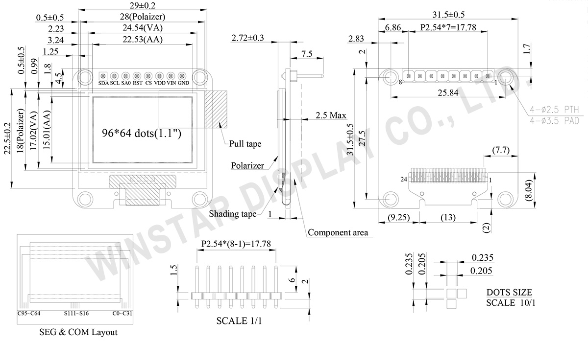
| No. |
符號 |
功能 |
| 1 |
SDA |
When serial interface mode is selected, D0 will be the serial clock input: SCLK; D1 will be the serial data input: SDIN.
When I2C mode is selected, D2, D1 should be tied together and serve as SDAout, SDAin in application and D0 is the serial clock input, SCL. |
| 2 |
SCL |
| 3 |
SA0 |
In I2C mode, this pin acts as SA0 for slave address selection.
When 3-wire serial interface is selected, this pin must be connected to VSS. |
| 4 |
RST |
This pin is reset signal input. When the pin is pulled LOW, initialization of the chip is executed.
Keep this pin HIGH (i.e. connect to VDD) during normal operation. |
| 5 |
CS |
This pin is the chip select input. (active LOW). |
| 6 |
VDD |
3.0V Power supply pin for core logic operation. |
| 7 |
VIN |
5.0V Power supply pin for core logic operation. |
| 8 |
GND |
This is a ground pin. |