


Chip on Glass LCD Module 240x128 with PCB
Model No. WO240128B2
►COG LCD
►Graphic LCD
►240 x 128 dots
►Built-in controller ST7586S
►3.3V power supply
►1/128 duty cycle
►Interface : Default 6800, Option 8080, SPI-4 Line/SPI-3Line 9bit
DESCRIPTION
WO240128B2 model is a COG LCD display WO240128B model with a PCB board on module, which is made of 240x128 dots. WO240128B2 is built in with ST7586S controller IC; it supports 6800 8-bit (default), 8080 8-bit parallel and serial SPI interface, power supply voltage 3.3V, 1/128 duty, 1/12 Bias. The advantage of WO240128B2 is having circuit layout on PCB board and with screw holes which make modules can be fixed on customers’ applications easily. Also, there are three kinds of connector pitch sizes of 2.54mm (default), 1.0mm and 0.5mm for options. WO240128B2 also have VDD 5V power supply voltage for optional.
This WO240128B2 module can be operating at temperatures from -20℃ to +70℃; its storage temperatures range from -30℃ to +80℃. The WO240128B2 is available for FSTN positive Transflective with white LED backlight. Please contact us if you need different types of LCDs or LED combinations.
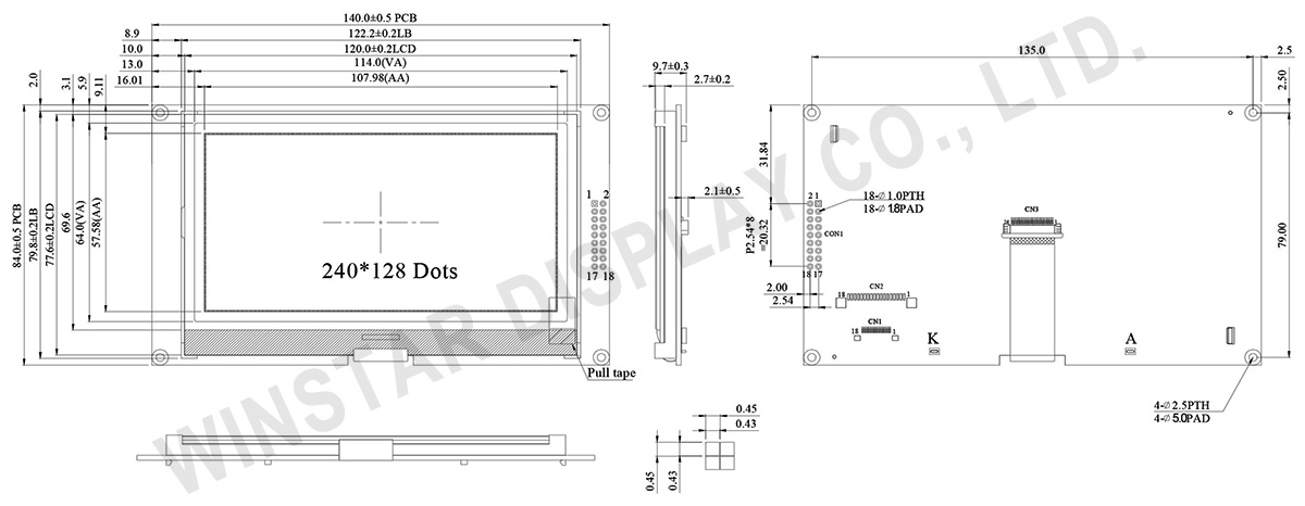
DRAWING
SPECIFICATIONS
Interface Pin Function
| Pin No. | Symbol | Description | |||||||||
|---|---|---|---|---|---|---|---|---|---|---|---|
| 1 | VDD | Power supply | |||||||||
| 2 | NC | No connection | |||||||||
| 3 | VSS | Ground | |||||||||
| 4 | CSB | Chip select input pin CSB=“L”: This chip is selected and the MPU interface is active CSB=“H”: This chip is not selected and the MPU interface is disabled (D[7:0] are high impedance) |
|||||||||
| 5 | RSTB | Reset input pin. When RSTB is “L”, internal initialization procedure is executed | |||||||||
| 6 | /RD(E) | Read / Write execution control pin. (This pin is only used in parallelinterface)
|
|||||||||
| 7~14 | D7~D0 | The bi-directional data bus of the MPU interface. When CSB is “H”, they are high impedance If using serial interface: D0 is the SDA signal in 4-Line & 3-Line interface D1 is the A0 signal in 4-Line interface |
|||||||||
| 15 | /WR/(R/W) | Read / Write execution control pin. (This pin is only used in parallel interface)
|
|||||||||
| 16 | A0(SCL) | The function of this pin is different in parallel and serial interface In parallel interface: A0 is register selection input A0 = "H": inputs on data bus are display data A0 = "L": inputs on data bus are command In serial interface: this pad will be used as SCL (serial-clock) input |
|||||||||
| 17 | A | LED+ | |||||||||
| 18 | K | LED- |
Mechanical Data
| Item | Dimension | Unit |
|---|---|---|
| Number of dots | 240 × 128 | - |
| Module dimension | 140.0 × 84.0 × 9.7 | mm |
| View area | 114.0 × 64.0 | mm |
| Active area | 107.98 × 57.58 | mm |
| Dot size | 0.43 × 0.43 | mm |
| Dot pitch | 0.45 × 0.45 | mm |
| Drive Method | 1/128 Duty,1/12 Bias | |
| Backlight Type | LED | |
| IC | ST7586S | |
Absolute Maximum Ratings
| Item | Symbol | Min | Typ | Max | Unit |
|---|---|---|---|---|---|
| Operating Temperature | TOP | -20 | - | +70 | ℃ |
| Storage Temperature | TST | -30 | - | +80 | ℃ |
| Digital Power Supply Voltage | VDDI | -0.3 | - | 3.6 | V |
| Analog Power supply voltage | VDDA | -0.3 | - | 3.6 | V |
| LCD Power supply voltage | V0-XV0 | -0.3 | - | 19 | V |
| LCD Power supply voltage | VG | -0.3 | - | 5.5 | V |
Electrical Characteristics
| Item | Symbol | Condition | Min | Typ | Max | Unit |
|---|---|---|---|---|---|---|
| Supply Voltage For Logic | VDD-VSS | - | 3.0 | 3.3 | 3.6 | V |
| Supply Voltage For LCM | VOP | Ta=-20℃ Ta=25℃ Ta=+70℃ |
- 14.8 - |
- 15.0 - |
- 15.2 - |
V V V |
| Input High Volt. | VIH | - | 0.7VDD | - | VDD | V |
| Input Low Volt. | VIL | - | VSS | - | 0.3 VDD | V |
| Output High Volt. | VOH | - | 0.8 VDD | - | VDD | V |
| Output Low Volt. | VOL | - | VSS | - | 0.2VDD | V |
| Supply Current | IDD | VDD=3.3V | - | 2.0 | 4.0 | mA |
Search keyword: 240x128 lcd, 240 x 128 lcd, lcd 240x128, lcd 240 x 128


