


产品叙述
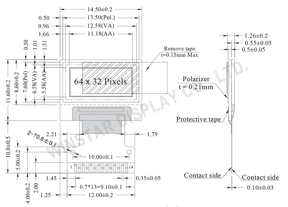
WEO006432A是一款0.49吋小尺寸单色被动式PMOLED显示器模组,解析度64x32 点阵。 WEO006432A模组尺寸为14.5x 11.6 x 1.26 mm, AA区尺寸为11.18 x 5.58 mm。 WEO006432A内建SSD1306 controller控制器, 模组支援传输介面I2C,使用3V电压驱动。此模组的工作温度是-40℃至+80℃,储存温度-40℃至+85℃。
WEO006432A为COG结构的OLED显示器模组,为有机自发光,无须背光源,模组轻薄且低耗电流,此款0.49吋OLED模组非常适合穿戴装置、手环、 MP3、 录音笔、小型手持式仪器、个人健康守护追踪装置等等。
规格图
产品规格
Pin功能定义
| No. | 符号 | 功能说明 |
|---|---|---|
| 1 | C2N | Positive Terminal of the Flying Inverting Capacitor Negative Terminal of the Flying Boost Capacitor The charge-pump capacitors are required between the terminals. They must be floated when the converter is not used. |
| 2 | C2P | |
| 3 | C1P | |
| 4 | C1N | |
| 5 | VBAT | Power Supply for DC/DC Converter Circuit This is the power supply pin for the internal buffer of the DC/DC voltage converter. It must be connected to external source when the converter is used. It should be connected to VDD when the converter is not used. |
| 6 | NC | No connection. |
| 7 | VSS | Ground of Logic Circuit This is a ground pin. It acts as a reference for the logic pins. It must be connected to external ground. |
| 8 | VDD | Power Supply for Logic This is a voltage supply pin. It must be connected to external source. |
| 9 | RES# | Power Reset for Controller and Driver This pin is reset signal input. When the pin is low, initialization of the chip is executed. |
| 10 | SCL | Host Data Input/Output Bus When serial mode is selected, D1 will be the serial data input SDIN and D0 will be the serial clock input SCLK. When I2C mode is selected, D2 & D1 should be tired together and serve as SDAout & SDAin in application and D0 is the serial clock input SCL. |
| 11 | SDA | |
| 12 | IREF | Current Reference for Brightness Adjustment This pin is segment current reference pin. A resistor should be connected between this pin and VSS. Set the current lower than 12.5μA. |
| 13 | VCOMH | Voltage Output High Level for COM Signal This pin is the input pin for the voltage output high level for COM signals. A capacitor should be connected between this pin and VSS. |
| 14 | VCC | Power Supply for OEL Panel This is the most positive voltage supply pin of the chip. A stabilization capacitor should be connected between this pin and VSS when the converter is used. It must be connected to external source when the converter is not used. |
规格说明
| 项目 | 尺寸 | 单位 |
|---|---|---|
| 点阵(分辨率) | 64 x 32 | Dots |
| 模块尺寸 | 14.5 × 11.6 × 1.26 | mm |
| 有效区域 | 11.18 × 5.58 | mm |
| 点间距 | 0.153 × 0.153 | mm |
| 点大小 | 0.175 × 0.175 | mm |
| 显示模式 | 被动矩阵 | |
| 显示颜色 | 单色 | |
| 驱动方式 | 1/32 Duty | |
| IC | SSD1306 | |
最大绝对额定值
| 参数 | 符号 | 最小值 | 最大值 | 单位 |
|---|---|---|---|---|
| 逻辑电源电压 | VDD | 0 | 4 | V |
| 显示电源电压 | VCC | 0 | 15 | V |
| 工作温度 | TOP | -40 | +80 | °C |
| 储存温度 | TSTG | -40 | +80 | °C |
电气特性
| 项目 | 符号 | 条件 | 最小值 | 典型值 | 最大值 | 单位 |
|---|---|---|---|---|---|---|
| 逻辑电源电压 | VDD | - | 2.8 | 3 | 3.3 | V |
| 显示电源电压 | VCC | - | 7 | 7.5 | 7.8 | V |
| 输入高电压 | VIH | - | 0.8×VDD | - | VDDIO | V |
| 输入低电压 | VIL | - | 0 | - | 0.2×VDD | V |
| 输出高电压 | VOH | - | 0.9×VDD | - | VDDIO | V |
| 输出低电压 | VOL | - | 0 | - | 0.1×VDD | V |
| 50% Check Board operating Current | ICC | VCC=7.5V | - | 5 | 20 | mA |
Search keyword: 64x32 oled, oled 64x32, 0.49 oled, 0.49" oled, 0.49 吋 oled, oled 0.49, oled 0.49", 0.49寸oled, oled 0.49寸


