
 - WEA012832E")
 - WEA012832E")
 - WEA012832E")
 - WEA012832E")
 - WEA012832E")
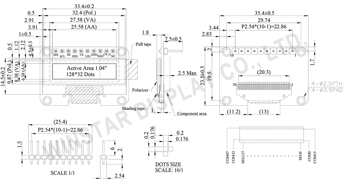
外形図
Data source ref: WEA012832EWPP3N00000
製品仕様
ピン功能定義
| No. | 記号 | 説明 |
|---|---|---|
| 1 | SDI | Serial data input This pin connects font IC of SDI and OLED drive IC of SDI. |
| 2 | SCL | Serial clock input This pin connects font IC of SCL and OLED drive IC of SCL. |
| 3 | DC | This is Data/Command control pin. |
| 4 | RES | This pin is reset signal input. When the pin is pulled LOW, initialization of the chip is executed. |
| 5 | CS | This pin is the chip select input. (active LOW). |
| 6 | VIN | Input voltage for 2.8 ~ 5.2V power supply. |
| 7 | GND | This is a ground pin. |
| 8 | SDO | Serial Data Output for font IC. Data is shifted out on the falling edge of the serial clock. |
| 9 | CS_G | Chip Select input for font IC. This pin is the chip select input. (active LOW). |
| 10 | NC | Not connection |
規格説明
| 項目 | 仕様 | 単位 |
|---|---|---|
| ドットマトリックス(解像度) | 128 x 32 | Dots |
| 外形寸法 | 35.4 × 23.5 × 1.8 | mm |
| 有効表示エリア | 25.58 × 6.38 | mm |
| ドットサイズ | 0.176 × 0.176 | mm |
| ドットピッチ | 0.200 × 0.200 | mm |
| 表示モード | パッシブマトリクス | |
| 発光色 | モノクロ | |
| 駆動方法 | 1/32Duty | |
| IC | SSD1306 | |
| Font IC | GT21L16T1W, オプションGT21L16S2W(簡体字中国語バージョン) | |
| インターフェイス | SPI | |
| サイズ | 1.04 インチ | |
絶対最大定格
| パラメーター | 記号 | 最小値 | 最大値 | 単位 |
|---|---|---|---|---|
| 入力電源電圧 | VIN | 2 | 7 | V |
| 操作温度 | TOP | -20 | +80 | °C |
| 保存温度 | TSTG | -40 | +85 | °C |
電気特性
| 項目 | 記号 | 条件 | 最小値 | 典型値 | 最大値 | 単位 |
|---|---|---|---|---|---|---|
| 入力電源電圧 | VIN | - | 2.8 | 3.0 | 5.2 | V |
| 入力電圧(High) | VIH | - | 2.4 | - | 3.2 | V |
| 入力電圧(Low) | VIL | - | 0 | - | 0.6 | V |
| 出力電圧(High) | VOH | - | 2.7 | - | 3.2 | V |
| 出力電圧(Low) | VOL | - | 0 | - | 0.3 | V |
| 50% Check Board operating Current | IIN | VIN=3V | - | 13.0 | 26.0 | mA |
")

 - WH1602A")
